Building semiconductor fabs is a complex and resource-intensive task. Traditional methods, where facilities are built entirely on-site, offer customisation but also come with long timelines, high costs, and limited flexibility. To meet the demands of rapid technological change, the industry is increasingly turning to preconstruction planning and prefabrication and modular (PFM) solutions.
Traditional Construction vs PFM Construction for Semiconductor Fabs
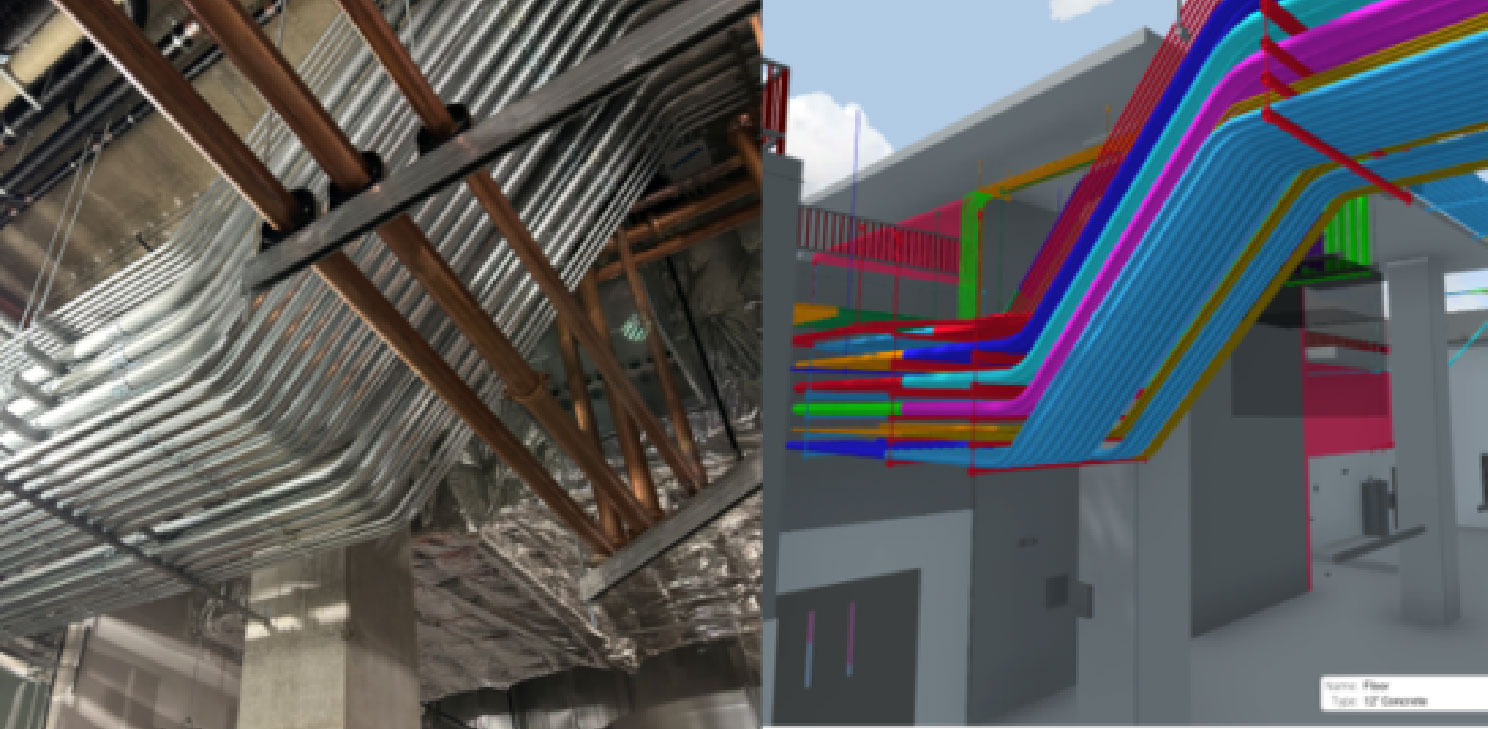
Historically, semiconductor fabs relied on custom on-site builds. While this approach delivered tailored cleanrooms and controlled environments, any changes or expansions required extensive downtime and resources. In contrast, modular cleanrooms and prefabricated units are manufactured off-site, then transported and assembled at the fab location. This shift has introduced new levels of speed, scalability, and cost efficiency, making it possible to keep pace with fast-moving production demands.
Benefits of Prefabrication and Modular (PFM) Solutions
- Faster and More Cost-Effective: PFM allows construction elements to be produced in controlled environments, often in locations with lower costs. With modules fabricated in parallel to site preparation, project timelines shorten significantly. Standardisation and reduced material waste further cut expenses.
- Improved Safety and Quality: By reducing reliance on on-site labour, PFM lowers safety risks during construction. Quality also benefits, since off-site assembly takes place under controlled factory conditions with tighter oversight.
- Sustainability Advantages: Construction waste is one of the largest contributors to global carbon emissions. Prefabrication can reduce material waste, optimise logistics, and even use renewable energy in off-site manufacturing. The result is a cleaner, more sustainable construction process with reduced impact on local ecosystems.
- Flexibility and Scalability: Modular designs can be reconfigured or expanded to meet new technological needs. Cleanrooms, skid-mounted utilities, or even structural components such as precast concrete and prefabricated steel can be swapped, upgraded, or scaled with less disruption than traditional builds.
Challenges of PFM in Semiconductor Construction
Despite its advantages, modular and prefabricated construction comes with hurdles. Managing multiple small manufacturing and construction sites introduces complex logistics and quality-control challenges. The return on investment can also be slow if the process is not standardised and integrated from the earliest stages.
To succeed, semiconductor companies need to:
- Introduce PFM concepts early in the construction process.
- Standardise practices across projects for consistency.
- Coordinate multiple teams—including contracting, logistics, supply chain, testing, and maintenance.
- Without early adoption and organisational alignment, the benefits of PFM can be harder to achieve.
A New Era for Fab Construction
The transition from traditional stick-built fabs to preconstruction planning and modular construction represents a fundamental change in semiconductor facility design. While challenges remain, the benefits in speed, safety, cost, and sustainability make the case clear. As companies adopt PFM more broadly, semiconductor fabs will become not only faster to build but also more adaptable and environmentally responsible—key factors in an industry that must constantly innovate to stay competitive.
To attend talks from industry leaders, connect with solution providers and network with peers, join us at the 2nd Constructing Sustainable Data Centers Europe: Revolutionizing Planning, Design, and Engineering, taking place on October 14-15, 2025, in Berlin, Germany.
For more information, click here or email us at info@innovatrix.eu for the event agenda. Visit our LinkedIn to stay up to date on our latest speaker announcements and event news.