The Constructing Semiconductor FAB Summit: Advances In Planning, Design And Engineering took place from June 11th to 12th in the bright and bustling tech hub of Austin, Texas, USA, with attendees from all over the semiconductor manufacturing and construction industries coming together at the Cambria Hotel Austin Downtown. The two day conference had a wide and comprehensive agenda that involved dozens of presentations from expert speakers, panel discussions, and networking breaks.
Our attendees explored the latest innovations in fab design, modular construction, cleanroom validation and humidity control, and sustainability, providing actionable insights to accelerate projects and reduce costs, leaving with the knowledge and connections to advance their projects and ensure that the U.S. remains a competitive leader in semiconductor manufacturing.
This article will provide a session recap for those who didn’t get the chance to attend and serve as a reminder for those who attended.
Constructing Capability: Facility Expansion in Active Semiconductor Fabs
William Groboski, Senior Facilities Engineer at Skywater Technology
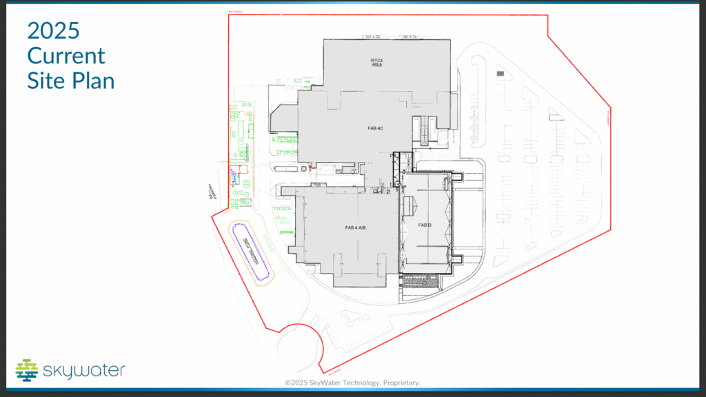
William spoke about successfully executing major construction projects without disrupting production, such as SkyWater Minnesota and SkyWater Florida. Facility expansion in the semiconductor industry typically means risk to production but SkyWater has proven that it is possible to expand and modernize active fabs without compromising output, with work that is on schedule, under budget, causes zero unplanned shutdown and doesn’t constrain production throughput. By using a small team so there was coordination between operations, construction and facilities and establishing protocols for airflow, particle control, and vibration mitigation, output was maintained during construction. He concluded by discussing how SkyWater’s expansion efforts prove that modernisation can occur inside active fabs and how investing in existing fabs is a faster and more sustainable path to readiness.
Fab Forward: AI/ML Innovations Transforming AEC in SemiFab Design and Delivery
Jim McCarthy, Technical Director-SemiFab EPC/ATF Facilities at Exyte
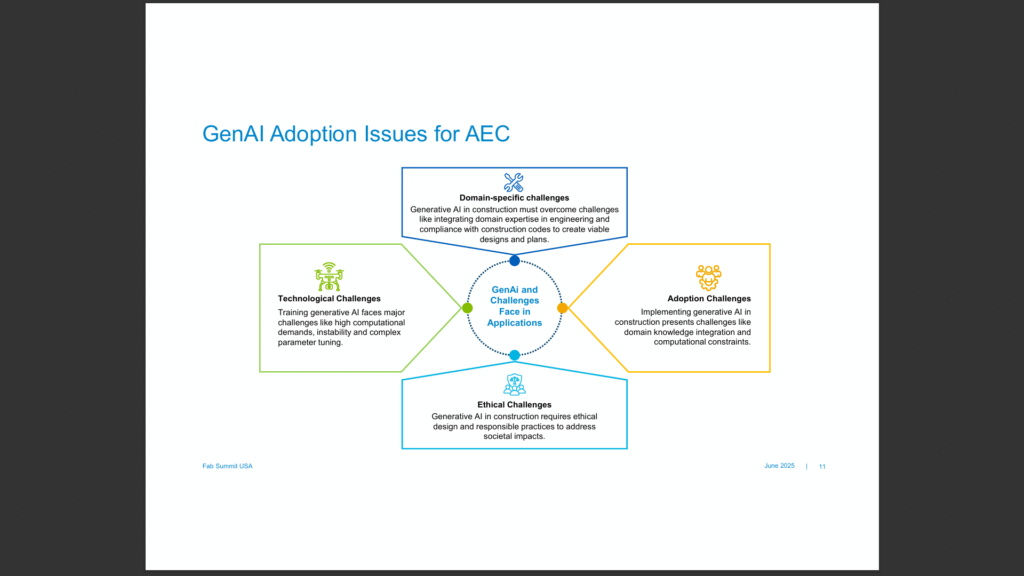
Jim shared his insights on how emerging digital technologies are reshaping facility design, construction, and operation. Generative AI enables rapid, data-driven design iterations that optimise layouts for cost, performance, and sustainability while integrating seamlessly with existing BIM and CAD systems. Digital twins provide real-time visibility and predictive analytics for proactive maintenance and operational efficiency. In construction, AI enhances scheduling and resource management, reducing delays and waste. Machine learning systems ensure environmental precision through continuous monitoring and adaptive control, supporting sustainability goals. Unified data platforms improve interoperability, eliminate silos, and allow scalable system integration. Predictive analytics further enable facilities to adapt to evolving needs, optimise lifecycle costs, and enhance resilience. Together, these innovations mark a shift towards intelligent, sustainable, and future-ready infrastructure.
Advantages of Design Build for Semi Conductor Facilities
Blake Hodess, Chief Executive Officer at Hodess Cleanrooms
Blake shared how a design-build, turn-key approach to cleanroom delivery offers a fully integrated solution that enhances efficiency, reduces costs, and mitigates risk for all stakeholders. Unlike traditional multi-vendor models that create friction and unclear accountability, design-build ensures a single point of responsibility from planning to maintenance. Early involvement of the cleanroom contractor enables seamless coordination, faster release of long-lead items, and proactive scheduling, resulting in shorter project timelines and earlier facility use. The integrated model eliminates cost overruns through design flexibility, streamlined communication, and shared project expertise. Experienced design-builders can provide a Guaranteed Maximum Price (GMP) early in the design phase, offering cost transparency and owner control over contingencies. Overall, this approach delivers greater certainty, efficiency, and value throughout the cleanroom project lifecycle.
Fab Facilities System Design Evolution and Current Practices
Pablo Ruiz, Regional Manager at Austin Commercial
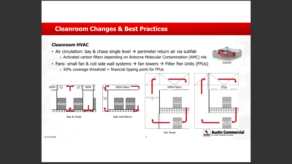
Pablo spoke about how, since the early 1990s, semiconductor manufacturing tools have evolved from smaller 5–6-inch systems with compact cleanroom footprints to larger, more complex 12-inch tools requiring extensive subfab support. Modern fabs now feature dual subfab levels clean and dirty—to accommodate increased tool density and utility demands. Cleanroom systems have advanced to meet these changing needs. Ceilings now use ISO 5 classifications with pleated PTFE filters, walkable T-grids, and integrated lighting for ease of maintenance. Raised metal floors made of aluminium range from 18” to 48” high, enhancing airflow and service access. HVAC systems employ Filter Fan Units, perimeter air returns, and dedicated makeup air units for precise environmental control. Supporting systems have also modernised: exhaust systems use efficient scrubbers and RCTO units; water and drain systems incorporate recycling and heat recovery; and process, chilled, and hot water systems utilise stainless-steel components, VFD-driven pumps, and energy-efficient cooling technologies to maximise sustainability and performance.
Enabling “fast-tracking” high tech fab construction projects to meet challenging customer demands
Jennifer Ahrens, Project Director at Sundt Construction
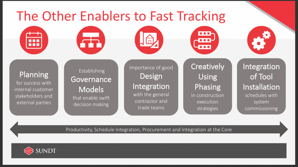
Jennifer shared her insights on how successful project delivery in advanced manufacturing depends on strong collaboration between internal stakeholders and external partners, anchored by senior leadership commitment and trust-building across all teams. Effective planning aligns construction and manufacturing priorities to meet factory need dates. A critical success factor is ensuring design integration—design packages should be *construction-optimised*, not just designer-optimised, with early and ongoing coordination between design, trade, and general contractor teams. Creative phasing strategies allow seamless integration of construction, facility operations, and tool installation, using phased areas, system start-ups, and commissioning sequences to maintain progress. Governance models featuring cross-functional leadership spanning owners, design, construction management, and operations—enable swift decision-making and proactive risk management. Finally, aligning **tool installation and system commissioning** around critical manufacturing qualification dates ensures that schedule priorities flow logically from end goals, driving timely and efficient project execution.
Addressing Environmental, Health & Safety (EHS) challenges for fab construction
Laurie S. Beu, Principal at Laurie S. Beu Consulting
Laurie discussed how semiconductor manufacturing relies on complex chemicals essential for producing nanoscale devices, but these materials present environmental and regulatory challenges. As new fabs are built for leading-edge production, suppliers must secure approval for new chemicals before start-up. During construction and equipment installation, fabs should enforce material declarations, minimise waste, segregate plastics like PVDF and PTFE, and pursue recycling or safe disposal. To reduce greenhouse gas emissions, the WSC Best Practice Guidance recommends process optimisation, replacing high-GWP gases, and using abatement systems and remote NF₃ cleans. PFAS, though critical for performance, pose significant environmental risks due to its persistence and toxicity. Suppliers must fully disclose any intentionally added or impurity-level PFAS, while fabs should test for emissions and install segregated exhaust and drainage for capture or abatement. Ultimately, industry-wide collaboration is vital—manufacturers, suppliers, and associations must coordinate on chemical regulation, disclosure, and safer innovation to ensure sustainable semiconductor production.
Just-in-time design. Forward-thinking delivery strategies in an evolving semiconductor industry
Andrew Jesaitis, Architectural SME, Advanced Technology at Arcadis
Andrew spoke about how the advanced manufacturing industry is defined by constant change, driven by innovations in AI, advanced packaging, photonics, and materials. To remain competitive, organisations must balance early definition of key elements such as functional areas, structural systems, and long-lead equipment with flexibility throughout design and implementation. This adaptability requires collaboration, open communication, and a willingness to explore unconventional solutions. As traditional project delivery models like Design-Bid-Build, Design-Build, and IPD evolve, teams must carefully manage risks and embrace new contracting strategies that prioritise integration and shared accountability. Expanding partnerships with contractors, specialist consultants, and vendors through off-site manufacturing, factory validation, and ongoing industry engagement enhances efficiency and innovation. Scaling delivery approaches according to project size ensures effective stakeholder representation, while embedding QA/QC processes from design through construction maintains quality and alignment. Ultimately, success in these unfamiliar landscapes depends on flexibility, collaboration, and a shared commitment to delivering future-ready facilities.
Best practices in project management for semiconductor facilities
Gregory Smith, Director of BIM/VDC at Yates Construction
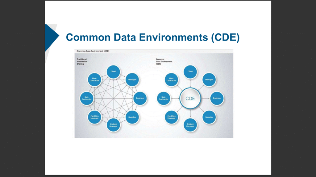
Gregory shared his knowledge on how collaboration between designers, engineers, contractors, and operators relies on trust, transparency, and a shared sense of purpose. Building strong communication and community fosters alignment around common goals, ensuring every stakeholder contributes meaningfully to project success. Advanced tools such as Building Information Modelling (BIM) and project management software play a crucial role in synchronising schedules, optimising resources, and maintaining design accuracy emphasising the principle of “building what we model.” Coordinated work must take priority, with all teams using the correct and most current drawings. To mitigate risks, robust contingency planning and well-structured Common Data Environments (CDEs) are essential. When multiple CDEs operate in isolation, siloed information leads to rework, cost overruns, and delays. Shared data and connected workflows, by contrast, enable smoother change management, minimise errors, and enhance efficiency—demonstrating that open collaboration and integrated systems are key to successful project delivery.

Consider This When Designing and Building a Semiconductor Fab – A View From the Sustaining Engineering and Operations Team
Thomas Huang, Senior Director of Engineering and Operations F8/F9 at GlobalFoundries

Thomas shared how GlobalFoundries operates manufacturing sites in Malta (NY), Singapore, Dresden (Germany), and Burlington (VT), and is expanding its U.S. operations with a strong focus on sustainability. The company aims to be carbon neutral and achieve net-zero emissions by 2050. By 2025, it targets reductions of 34% in electricity use intensity, 26% in water use intensity, and 16% in total waste intensity compared to 2020 levels. GF’s strategy emphasises early and continuous involvement of operations teams during design, balancing environmental, safety, reliability, cost, and schedule priorities. Flexibility in design, effective change management, and thorough commissioning are key, alongside renewed collaboration to address environmental challenges such as PFAS and PFOA.
Protocol Management in a Semi-Conductor Construction Project
Erika Hodess, CEO of PMS LLC/Vice President of Services at Hodess Cleanrooms
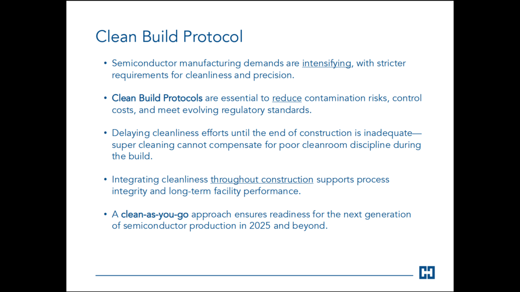
Erika spoke about how a clean build protocol during semiconductor facility construction is vital to prevent contamination, control costs, and comply with strict regulations. Cleanliness must be integrated from the outset, as end-of-project cleaning cannot make up for poor practices during construction. Adopting a “clean-as-you-go” approach ensures long-term process integrity and prepares facilities for advanced semiconductor production in 2025 and beyond. Real-time monitoring software now enables tracking of particle counts, temperature, and humidity throughout construction, allowing immediate corrective action. Additionally, advanced sensors can measure particulate matter and volatile organic compound (VOC) levels, helping assess filtration efficiency, detect unsuitable materials, and maintain the required cleanliness standards essential for semiconductor manufacturing performance.
Operations Challenges and Opportunities in Legacy Semiconductor Manufacturing Facilities
Nathan Roisen, Principal – Science & Technology Practice Lead, and Chris Fischer, Architect, at BWBR
The pair from BWBR spoke to our delegates about how, whilst the semiconductor industry often focuses on large-scale new projects, many manufacturers still rely on valuable legacy facilities, some of which are decades old. The presentation explores strategies to extend the lifespan and productivity of these older sites through targeted investments. Legacy facilities face unique design challenges across various disciplines including zoning and site functionality (civil), utility routing (structural), wafer transport and code compliance (architectural), HVAC and airflow management (mechanical), and equipment lead times and power capacity (electrical). Even modest upgrades can deliver substantial benefits, such as increased capacity, improved redundancy, enhanced equipment distribution, and optimised workflow efficiency, ultimately helping legacy operations remain competitive and valuable for years to come.
From Microns to Nanometers: The IRDS and Addressing New Challenges in Micro-Contamination Control
Chris Muller, Director IEQ Technical Services, at AAF International
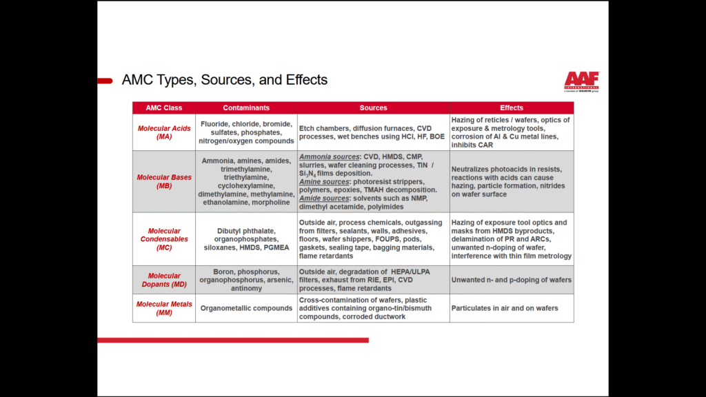
Chris shared how, as semiconductor device dimensions continue to shrink, the proportion of process steps affected by molecular or non-particulate contamination is rising, making airborne molecular contamination (AMC) increasingly harmful to wafer processing. Efforts to control AMC began with the International Technology Roadmap for Semiconductors (ITRS), evolved through the International Roadmap for Devices and Systems (IRDS), and continue to adapt for future manufacturing needs. Modern countermeasures now focus on advanced solutions such as minienvironments and specialised chemical filtration systems. These are designed to target and remove specific contaminants based on identified AMC species, making comprehensive and tailored filtration strategies essential for maintaining quality and reliability in cutting-edge semiconductor fabrication facilities.
Water Management in Semiconductor Fab Construction: Strategies for Sustainability, Efficiency, and Risk Mitigation
Kelly Osborne, Fab Facilities Operations Sr. Staff Engineer, at Intel Corporation
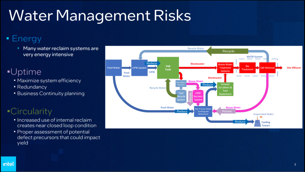
Kelly spoke to our audience about how the semiconductor industry faces growing sustainability challenges as more complex chip designs demand additional process layers, increasing water and energy consumption. Facilities must maintain 100% uptime while reducing their environmental impact and ensuring operational efficiency. To address these pressures, the goal is to achieve net positive water by 2030, conserving 60 billion gallons through internal savings and external restoration projects. Strategies include water reuse, reclamation, and recycling across ultrapure water (UPW) and facility systems, recovering rinse water, and treating wastewater on- or off-site. Collaboration with suppliers, industry partners, and municipalities is essential to improve water efficiency, integrate reuse into tool design, and strengthen water infrastructure. Advanced monitoring technologies and planning further support water conservation and business continuity.
Seeing from both sides: Lessons from a career as an owner and a GC
Matt Cannon, Regional Manager Advanced Technologies at Austin Commercial
Matt discussed how both general contractors (GCs) and owners play vital roles in the expanding U.S. semiconductor manufacturing sector, which now demands more fabs and R&D facilities. GCs value clear planning, strong partnerships, and decisive leadership from owners, while owners expect open communication, an understanding of the fab’s purpose, and a willingness to adopt new technologies. The industry’s future success depends on forming landmark partnerships built on trust, collaboration, and innovation. By fostering transparent communication and a shared commitment to efficiency and technological advancement, both parties can deliver the next generation of domestic semiconductor facilities effectively and sustainably.
Navigating the Compliance Landscape: Strategies for Fab Expansion
Becky Kim, Environmental Engineer at Microchip Technology
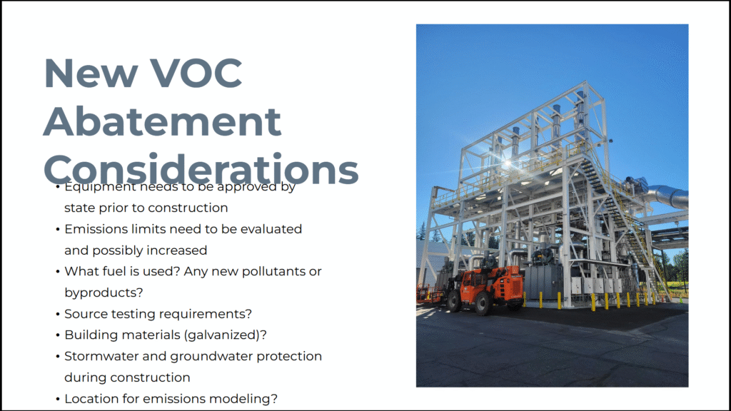
Becky shared how during semiconductor facility expansion, environmental compliance presents several challenges, particularly under the Clean Air Act, which aims to protect public health through strict air quality regulations. Facilities must comply with both risk-based and technology-based standards, as well as obtain construction (New Source Review) and operating (Title V or Non-Major Source) permits. Sites located in nonattainment areas that exceed EPA air quality standards face more stringent requirements. Expansion often introduces new chemicals, processes, or increased production, all of which can raise emissions and require updated permits or added abatement systems. Even temporary equipment must be accounted for. Additionally, evolving state regulations, extended permitting timelines, and higher costs complicate compliance, making proactive planning and close regulatory coordination essential. Becky discussed a case study on VOC abatement and the lessons learned from locating its 3 RCTOs, with a final location in the courtyard with stacks built tall to help with air dispersion and odour.
Bridging the Workforce Gap in Semiconductor Fab Construction
Dr. Steve Putna, Associate Vice Chancellor for Research and Director of the Texas A&M Semiconductor Institute at The Texas A&M University System
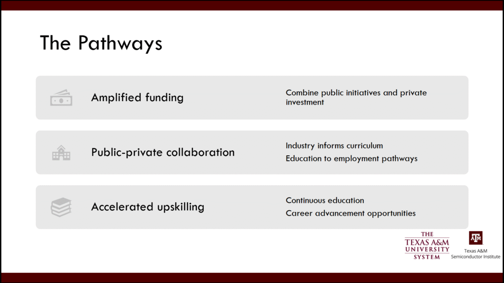
Dr Putna spoke to our delegates about how the semiconductor industry faces a critical labour shortage, with high turnover, rising costs, and delayed projects due to a lack of skilled workers. Training gaps persist, as few programmes prepare professionals for the specialised requirements of semiconductor environments, leading to retention issues and limited career growth. Intense competition for talent across industries further drives up recruitment costs. To address these challenges, the sector must invest in education and training, partnering with universities and technical schools to develop targeted programmes. Public-private collaboration, supported by initiatives like the CHIPS Act, can fund workforce development, while upskilling and reskilling existing workers will help fill key roles. Long-term success depends on joint efforts between industry, government, and the education sectors.

Execution EPC&M Plan for A Semiconductor Production MODULE PLANT
Julian Helmi, CTO/Founder of Prime Construction USA
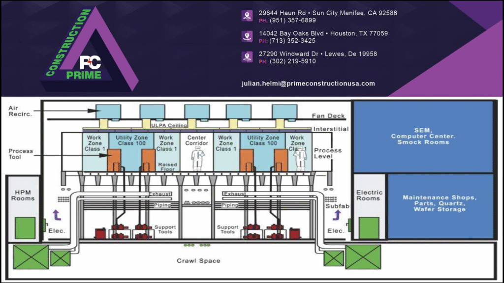
Julian spoke about how a typical EPC&M (Engineering, Procurement, Construction, and Management) project for MEP-based facilities such as data centres, pharmaceutical plants, EV battery sites, or semiconductor fabs focuses on the design, construction, and commissioning of advanced infrastructure. Effective project management involves detailed planning, budgeting, scheduling, and resource allocation across five key phases: Pre-Construction, Procurement, Construction, Testing and Commissioning, and Handover/Close-out. To mitigate risks and ensure efficiency, teams implement AI-driven predictive maintenance, strengthen supply chains through strategic partnerships, and adopt modular design for flexibility. Additional strategies include using digital twins for process optimisation, investing in energy-efficient technologies, and applying data-driven forecasting to streamline inventory and enhance overall project resilience and performance.
From Chaos to Control: How Project Controls Transform Construction Efficiency
Matt Johnson, Sr. Project Manager at JE Dunn Construction
Matt shared his insights on how large-scale industrial projects involve significant complexity, with multiple stakeholders, shifting regulations, global supply chain risks, and unpredictable site conditions. To address this, an integrated systems approach combines cost control, scheduling, risk management, and quality assurance frameworks. Effective planning includes detailed work breakdowns, realistic schedules, and budgets with contingencies. Structured change management ensures proper documentation, stakeholder review, and controlled implementation. A systematic risk management process identifies, quantifies, and monitors potential issues, supported by contingency plans. Productivity is maximised through resource coordination, lean construction, and preventive maintenance. Digital tools such as project management software, mobile data apps, IoT-enabled dashboards, and predictive analytics enhance control and visibility. These systems enable measurable improvements in time, cost, and quality, ensuring transparent performance tracking across all phases.
Optimizing Fab Construction with AI-Driven Scheduling
Kevin Fuller, Director of Industrial Solutions at ALICE Technologies
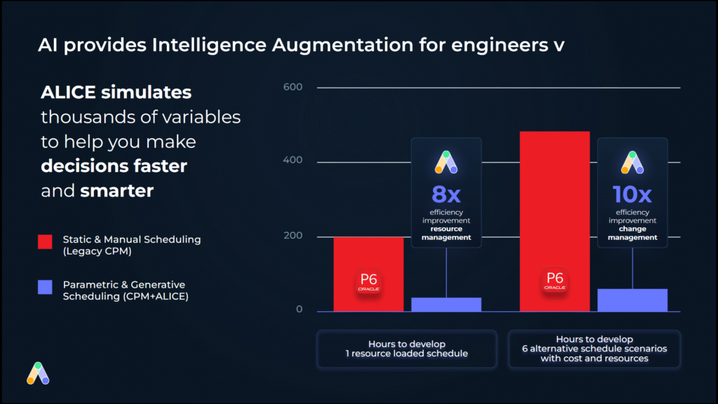
Kevin spoke to our audience about how semiconductor fabrication projects, rigid and highly detailed schedules can make plans fragile and vulnerable to disruption. To overcome this, project teams are adopting antifragile approaches and methods that strengthen performance under uncertainty. By rapidly simulating delays, disruptions, and “what-if” scenarios, teams can identify risk-reduced recovery solutions and adapt to macroeconomic challenges such as supply chain volatility. Tools like ALICE, a generative scheduling platform, enable the rapid exploration of multiple construction sequences and variables, helping determine the most efficient execution path. This allows teams to automatically adjust plans during both design and construction phases, improving resilience, optimising timelines, and showcasing successful adaptation strategies from recent semiconductor fab projects.
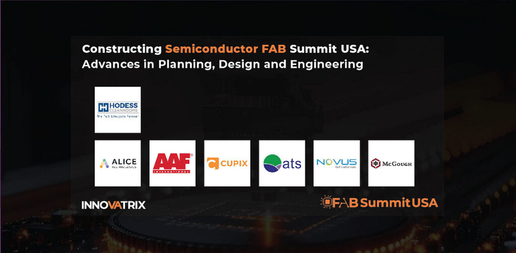
Sponsors
The Constructing Semiconductor FAB Summit USA was supported by a wide range of sponsors who brought their teams to our exhibition hall, and Innovatrix would like to thank them again for their support.
If you would like to network with fellow experts and innovators from across the semiconductor manufacturing industry and be informed on the latest innovations in fab construction, join us at an Innovatrix conference today! Our next edition of the Constructing Semiconductor FAB Summit will be taking place next summer.
For more information, visit our website or email us at info@innovatrix.eu for the event agenda. Visit our LinkedIn to stay up to date on our latest speaker announcements and event news.