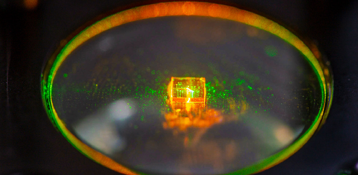
Entegris, Inc., a global leader in advanced materials science, in collaboration with the Trump Administration, today announced $700 million in domestic R&D spending over the next several years to accelerate semiconductor innovation. This investment in R&D projects and related capital expenditures will span its two divisions, Materials Solutions and Advanced Purity Solutions.
A portion of this investment will be used to develop its Aurora, Illinois location, strategically located between semiconductor hubs in New York, Ohio, Arizona and Texas, into a state-of-the-art U.S. Technology Center. This facility will be a cornerstone to Entegris’ solutions selling strategy focused on maximizing product performance and minimizing time to market, across its complete suite of solutions including its deposition materials, slurries, cleans, and CMP pads.
The investments in the U.S. will leverage a strong talent base and demonstrate Entegris’ commitment to supporting advanced semiconductor manufacturing and driving technology leadership. This investment complements Entegris’ previous commitment of $700 million to development of a state-of-the-art manufacturing center of excellence in Colorado Springs, CO.
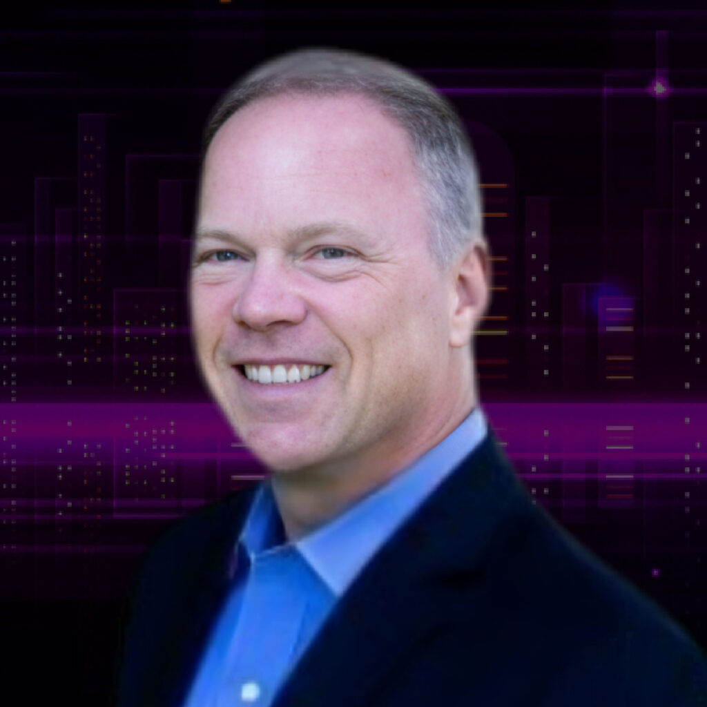
“To support the industry’s growth, we have been creating a stronger and more resilient domestic semiconductor ecosystem in the U.S.,” said Entegris president and CEO Dave Reeder. “These investments also allow for continued leadership in advanced materials solutions.”
As the semiconductor industry expands in the U.S., the need for new domestic capacity and additional collaboration on innovation will grow. Meeting these demand levels will create new opportunities for semiconductor materials suppliers to meet current and future needs.
Entegris’ move aligns with the broader trend of onshoring semiconductor capabilities amid growing global demand, geopolitical challenges, and supply chain vulnerabilities. The U.S. government’s support through initiatives like the CHIPS and Science Act has further encouraged industry players to reinvest in domestic infrastructure.
To find out more about the latest industry updates and innovations in semiconductor plant construction, meet with solution providers and hear talks from expert speakers, attend the 2nd Constructing Semiconductor FAB Summit Europe: Advances In Planning, Design And Engineering, taking place on October 21-22, 2025, in Munich, Germany.
For more information, click here or email us at info@innovatrix.eu for the event agenda. Visit our LinkedIn to stay up to date on our latest speaker announcements and event news.
Source: