The global race to build advanced chip manufacturing facilities has intensified, making semiconductor fab construction one of the most time-sensitive and capital-intensive projects in modern industry. Companies looking to bring new fabs online quickly must adopt smarter design approaches, advanced digital tools, and efficient construction strategies. Fast-tracking semiconductor fab construction is not simply about working faster—it requires strategic planning, coordinated execution, and the right expertise.
Below are key strategies that help accelerate semiconductor fab construction projects while maintaining quality and reliability.
Use Advanced Digital Tools to Improve Design and Planning
One of the biggest drivers of efficiency in semiconductor fab construction is the use of advanced digital tools during the design and planning stages. Traditionally, many projects rely on BIM 4D, which integrates 3D modeling with project scheduling. However, BIM 4D lacks the financial planning dimension that is critical for capital-intensive fab projects.
BIM 5D platforms provide a significant advantage by integrating cost management into design and scheduling. Tools such as RIB enable teams to combine 3D modeling, scheduling, and financial planning within a single environment. This improves project automation and allows stakeholders to immediately see how design changes affect construction schedules and costs.
The cost component also enhances visibility into material delivery milestones, including bill of materials references. As a result, project teams can manage cash flow more effectively—an essential capability in large-scale semiconductor fab construction.
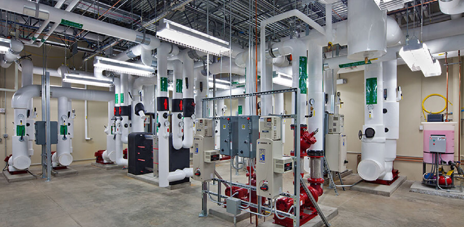
Optimize Power System Design with Specialized Software
Another major factor influencing project timelines is the design of the fab’s power system. During the early stages of semiconductor fab construction, engineers often focus heavily on mechanical and process systems. This sometimes leads to less time dedicated to electrical and power design, causing teams to reuse designs from previous projects.
While reusing designs may seem efficient, it can prevent manufacturers from optimizing their systems or meeting local standards when building fabs in new geographies.
Industry-leading software such as ETAP helps solve this challenge by enabling engineers to design, simulate, and optimize power system architectures. Using advanced simulation tools reduces design errors and ensures the electrical infrastructure meets the strict operational and quality requirements of semiconductor facilities.
Leverage Specialized Expertise
Digital tools alone are not enough to accelerate semiconductor fab construction. Expertise from experienced power systems specialists also plays a crucial role.
Expert groups with a history of supporting semiconductor manufacturers can contribute to areas such as medium- and low-voltage electrical distribution, secured power solutions, and power monitoring and automation. Through co-design collaboration, these specialists work directly with project teams to develop and optimize electrical distribution systems.
They can also provide reference designs, technical studies, and support workshops. Another important contribution is adapting existing designs to new standards when building fabs in different regions—for example, translating designs from IEC standards to NEMA standards when moving projects from Asia to the United States.
Adopt a Concept-First Design Philosophy
A common mistake in semiconductor fab construction is attempting to finalize every design detail before construction begins. This approach can delay projects by months or even years.
Many advanced fabs instead adopt a concept-first design philosophy. Teams define process requirements, create high-level facility concepts, hire contractors early, and allow detailed engineering to continue during construction. By avoiding the need to finalize 100% of the design upfront, projects can move to the construction phase much sooner.
Rely on Contractor-Led Design
Specialized semiconductor facility contractors often have extensive experience in cleanroom architecture, subfab layouts, and tool utility requirements. Relying on these contractors for design and execution can significantly accelerate semiconductor fab construction.
Contractors who have delivered multiple fabs understand the complexities of semiconductor facilities and can implement proven solutions quickly. Rather than relying solely on consultants, engaging experienced contractors early helps streamline the project.
Execute Tasks in Parallel
Parallel execution is another powerful strategy for fast-tracking semiconductor fab construction. Instead of performing tasks sequentially, multiple activities can occur simultaneously. This approach can reduce project timelines by six months to a year compared to slower models where tasks occur one after another.
Manage Procurement and Supply Chains Strategically
Procurement is often a major source of delays in semiconductor fab construction. Critical equipment such as transformers and chillers can take six to twelve months to arrive. Ordering long-lead equipment early—even before final design completion—can help projects avoid supply bottlenecks.
Strong local supply chains also reduce delays by ensuring access to cleanroom panels, gas systems, facility modules, and specialized contractors without relying on imports.
Monitor Progress and Plan for Risks
Finally, effective planning and monitoring are essential. Project teams should identify potential bottlenecks early, develop contingency plans for delays or regulatory changes, and continuously monitor progress against the project schedule.
Analyzing past project data through techniques such as reference class forecasting can help teams anticipate risks and make more accurate planning decisions.
Conclusion
Fast-tracking semiconductor fab construction requires more than aggressive schedules. It demands the right combination of digital tools, specialized expertise, streamlined design strategies, and efficient procurement practices. By integrating advanced modeling technologies, leveraging experienced contractors, and executing tasks in parallel, manufacturers can significantly shorten timelines and bring new fabs online faster.
In the semiconductor industry, speed is rarely accidental—it is the result of carefully engineered strategies, strong ecosystems, and disciplined project execution.
To discuss semiconductor manufacturing, fab construction and key issues facing the industry, connect with solution providers and network with delegates, attend the 3rd Constructing Semiconductor FAB Summit USA: Advances in Planning, Design and Engineering, taking place June 24-25, 2026, in Austin, Texas, USA.
For more information, click here or email us at info@innovatrix.eu for the event agenda. Visit our LinkedIn to stay up to date on our latest speaker announcements and event news.