The European Chips Act will bolster Europe’s competitiveness and resilience in semiconductor technologies and applications, and help achieve both the digital and green transition. It will do this by strengthening Europe’s technological leadership in the field. Following the approval by the Parliament and the Council, the regulation entered into force on 21 September 2023.
Semiconductor shortages forcing factory closures made the extreme global dependency of the semiconductor value chain on a very limited number of actors in a complex geopolitical context more evident. The findings of the Chips Survey, launched by the European Commission, highlighted that industry expects demand for chips to double by 2030. This reflects the growing importance of semiconductors for European industry and society. In her 2021 State of the Union speech, Commission President Ursula von der Leyen set the vision for Europe’s chip strategy, to jointly create a state-of-the-art European chip ecosystem. This will include production, as well as connecting the EU’s world-class research, design and testing capacities.
With the European Chips Act, the EU will address semiconductor shortages and strengthen Europe’s technological leadership. It will mobilise more than €43 billion of public and private investments and set measures to prepare, anticipate and swiftly respond to any future supply chain disruptions, together with Member States and international partners.
This will be achieved based on three pillars of action:
- The “Chips for Europe Initiative” will support large-scale technological capacity building and innovation
- A framework to incentivise public and private investments in manufacturing facilities will ensure the security of supply and resilience of the Union’s semiconductor sector
- A coordination mechanism through the European Semiconductor Board will be the key platform for coordination between the Commission, Member States and stakeholders
The Chips Act itself should result in additional public and private investments of more than €15 billion. These investments will complement existing programmes and actions in research and innovation in semiconductors, such as Horizon Europe and the Digital Europe programme and announced support by Member States.
I – Chips for Europe
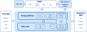
Pillar I of the European Chips Act establishes the Chips for Europe Initiative, which has the objective of supporting technological capacity building and innovation in the Union by bridging the gap between the Union’s advanced research and innovation capabilities and their industrial exploitation. To this end, the Chips for Europe Initiative has the following five operational objectives:
- Setting up a Design Platform
- Enhancing existing and developing new advanced pilot lines
- Building capacities for accelerating the development of Quantum chips and associated semiconductor technologies
- Establishing a network of competence centres across the Union
- Setting up a Chips Fund to facilitate access to debt financing and equity, in particular for start-ups, scale-ups, SMEs and small mid-caps
II – Security of supply and resilience
Pillar II of the European Chips Act sets up a framework to ensure the security of supply and resilience of the Union’s semiconductor sector by attracting investments and enhancing production capacities in manufacturing, advanced packaging, test, and assembly. The two main elements of Pillar II are:
- Status of integrated production facility and open EU foundry
- Characteristics of IPFs and OEFs
- Application and guidance
- Benefits and obligations
- Label of design centre of excellence
- Characteristics of design centres of excellence
- Requirements and application for the label
III – Monitoring and crisis response
Pillar III of the European Chips Act establishes a coordination mechanism between the Member States and the Commission to strengthen collaboration on monitoring and crisis response. An overview of Pillar III coordination mechanism would be:
- Monitoring
- Strategic mapping
- Early-warning indicators
- Key market actors
- Risk mitigation
- Crisis response
- Activation of the crisis stage
- Emergency toolbox
- Information gathering
- Priority-rated orders
- Common purchasing
- Governance
- European Semiconductor Board
To discuss the latest innovations and developments in semiconductor manufacturing, network with peers and solution providers and attend talks from industry leaders, book your place to attend the 2nd Constructing Semiconductor FAB Summit Europe: Advances In Planning, Design And Engineering, taking place on October 21-22, 2025, in Munich, Germany.
For more information, click here or email us at info@innovatrix.eu for the event agenda. Visit our LinkedIn to stay up to date on our latest speaker announcements and event news.
Source: