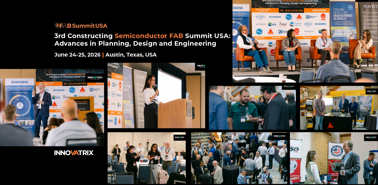
Innovatrix returned to the Lone Star State this year with our event, the 3rd Constructing Semiconductor FAB Summit USA: Advances in Planning, Design and Engineering that took place June 24-25, 2026, at the HiltonAustin Airport Hotel inAustin, Texas, USA.
The exclusive two-day event brought together industry leaders, engineers, EPCs, technology providers, and policymakers to explore the latest innovations in fab design, modular construction, cleanroom validation, humidity control, and sustainable engineering practices.
Our audience gained insights into next-generation facility Semiconductor Facility Design, design, advanced engineering methodologies, and digital tools supporting fab construction. The tradefair showcased cutting-edge solutions for Semiconductor Cleanroom systems, modular building techniques, advanced materials, energy-efficient infrastructure, and process integration technologies that enable faster, more resilient fab development.
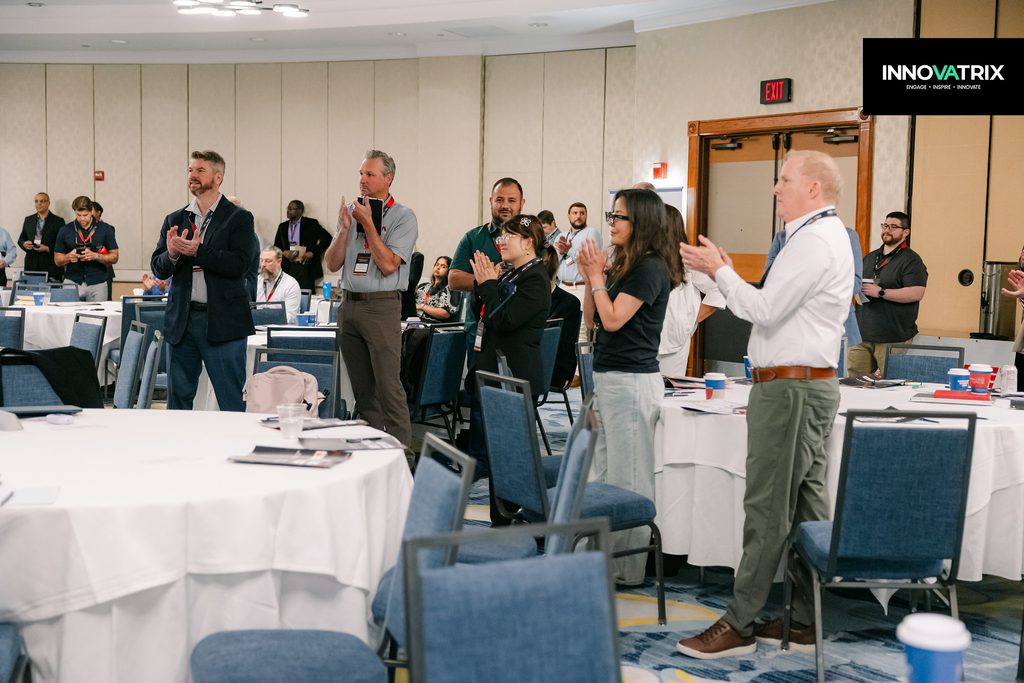
This article will provide a session recap for those who didn’t get the chance to attend and serve as a reminder for those who attended.
Building with Integrity: Keeping Ethics at the Core of Complex Construction Projects
Valentina K. Sabet, Governance, Risk & Operational Audit – Foundry Construction & Sourcing at Intel Corporation

Valentina emphasized that ethics is a shared responsibility across the construction project ecosystem and a critical factor in successful project delivery. With construction among the industries most vulnerable to fraud, semiconductor megaprojects face additional risks due to multibillion-dollar budgets, compressed schedules, complex subcontracting chains, accelerated procurement decisions, and public incentives. She highlighted common ethical pressure points, including bid rigging, conflicts of interest, safety and quality shortcuts, inflated change orders, inaccurate reporting, and labor exploitation. These issues often begin as small compromises that become normalized over time. Drawing on case studies from Brazil and the UK, she demonstrated how collusion between owners and contractors damages market integrity and affects the wider supply chain. She also outlined early warning signs, such as unexplained procurement decisions, undocumented payments, inconsistent reporting, and limited supplier transparency. To help organizations manage these risks, she introduced the 3C framework: Clarity in contractual expectations and responsibilities, Consistency in applying ethical standards across all partners, and Courage to speak up and escalate concerns. She concluded that ethical culture is shaped by everyday leadership decisions and behaviors, making integrity not simply a compliance requirement but a prerequisite for successful project execution.
Semiconductor Virtual Factory – Information Foundations
Michael Potts, Director of Architecture & Engineering at Arcadis

Michael explored the importance of accurate, timely information in establishing semiconductor Virtual Factory digital twins that support stakeholders throughout a facility’s lifecycle. He explained how digital representations of fab environments can integrate planning, engineering, construction, scheduling, procurement, commissioning, asset management, facilities management, and manufacturing systems. However, manufacturing equipment remains a significant gap, as equipment vendors are often reluctant to share 3D models due to intellectual property concerns, while available models can be expensive or fail to meet customer requirements. To address these challenges, he highlighted the SEMI Manufacturing Equipment Installation Task Force and the newly published SEMI F122 guide, which establishes requirements for Facilities Data Packages (FDPs). These packages comprise 3D equipment models, 2D installation templates, and detailed data sheets covering equipment dimensions, clearances, utility connections, and installation requirements. The guidance provides standardized formats and specifications to improve consistency and information exchange between equipment suppliers and fab owners without requiring the disclosure of proprietary information. Michael concluded that semiconductor manufacturers should incorporate clear Virtual Factory digital twin deliverables into procurement contracts, using established SEMI standards to ensure accurate equipment and facilities data is available when needed throughout the project lifecycle.
Computational Fluid Dynamics in Semi
Blake Hodess, CEO of Hodess Cleanrooms

Blake examined the role of Computational Fluid Dynamics (CFD) modeling in semiconductor manufacturing, highlighting its value in simulating airflow, thermal conditions, contaminant dispersion, and indoor air quality under different air distribution configurations. He explained that CFD simulations rely on accurate input data and modeling assumptions, meaning their results should be treated as design aids for comparing alternatives rather than exact predictions of real-world conditions. Key inputs include supply and return air locations and velocities, equipment dimensions and heat loads, and exhaust locations and velocities. He outlined three important applications of CFD in semiconductor facilities. First, heat load management uses temperature maps and heat flux distributions to identify potential hotspots, optimize cooling strategies, and improve equipment reliability. Second, manufacturing and equipment optimization examines airflow distribution, pressure fields, and particle trajectories to improve wafer-level process uniformity and optimize deposition and etch chamber airflow. Third, contamination control uses airflow visualization and particle tracking to reduce particle accumulation, optimize cleanroom airflow patterns, and balance cleanliness requirements with energy efficiency. Blake highlighted how CFD can support more reliable, efficient, and precisely controlled semiconductor manufacturing environments.
From Silicon to Structure: Digital Delivery in Semiconductor Facilities
Sindhu Gundimeda, Director of Construction Technologies, and Enrique Sarmiento, VDC Manager II, at Austin Commercial

Sindhu and Enrique explored how digital delivery strategies can improve coordination, efficiency, and project outcomes in complex semiconductor facility construction. They identified four key challenges across the project lifecycle: communication barriers between geographically dispersed teams, accelerated construction schedules, demanding spatial and tolerance requirements, and inconsistencies in BIM data maturity. To address communication challenges, they highlighted the value of a Common Data Environment (CDE) as a centralized source of project information, supported by physical colocation to enable real-time problem-solving and faster RFI responses. For accelerated timelines, they demonstrated how 4D logistics, integrated construction schedules, and visual supply chain dashboards can improve long-lead equipment tracking and coordinate complex site activities. They also emphasized space management, automated clash detection, and regular laser scanning to identify structural deviations before they affect construction. Addressing BIM maturity gaps requires early collaboration between trade partners and design teams to develop coordinated models that evolve throughout the project lifecycle while preserving critical asset information for operations. Finally, they discussed emerging applications of AI for automated drawing, specification, and schedule audits, with secure internal environments protecting sensitive data. They concluded that integrating digital tools with strong collaboration across owners, designers, and contractors supports more predictable delivery, cost control, and successful operational digital twins.
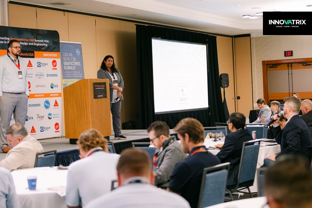
Clean & Dry Rooms: When Walls and Ceilings Become High- Sensitivity Engineering Systems
Tobias Frieser, Business Development Manager EU & USA at Pophen

Tobias discussed how modular construction can improve the delivery of clean and dry rooms in semiconductor facilities, where walls and ceilings must meet demanding engineering, safety, and quality requirements. He highlighted the limitations of traditional construction methods, including sequential processes, weather dependency, labor-intensive installation, longer delivery times, and increased costs and project risks. Modular systems offer an alternative through parallel execution, factory-based manufacturing, controlled production environments, and faster on-site assembly. By starting manufacturing once designs reach approximately 60% completion, components can be produced while other construction activities continue. Pre-packaged deliveries, organized according to installation sequence, also eliminate unnecessary storage and reduce time spent locating materials. Tobias explained that this approach can reduce the time from design to construction readiness by approximately 50%, while lowering labor costs, on-site waste, and installation adjustments. He also emphasized the importance of factory inspections and quality testing to ensure components meet project requirements before delivery. With multiple international certifications and approvals, modular systems provide greater quality control, schedule certainty, and reduced construction risk. He concluded that modular construction can help semiconductor manufacturers accelerate facility delivery while maintaining better control over costs, labor, and project execution.
The Fab Is the Easy Part: Creating the One-Team Environment Behind Mega Project Success
Matt Gulley, Vice President & General Manager – Semiconductor at Turner Construction

Matt examined why large-scale semiconductor projects frequently exceed their budgets and schedules, emphasizing that technical construction is only one part of successful megaproject delivery. He highlighted research showing that just 8.5% of megaprojects finish on budget and on time, while only 0.5% achieve their expected benefits as well. Drawing on the scale of CHIPS Act investments, he explored common causes of project failure, including optimism bias, inadequate front-end planning, weak governance, adversarial procurement models, leadership instability, organizational silos, and poor coordination between contractual and technical interfaces. He outlined several ways to improve project outcomes, including stronger project definition, independent forecasting, integrated owner-designer-builder teams, aligned commercial incentives, shared project data, and faster decision-making. A central theme was the importance of psychological safety and team culture. He explained that effective teams need a shared sense of purpose, clear responsibilities, dependability, and an environment where people can raise concerns, challenge assumptions, and admit mistakes without fear of blame. He also emphasized the importance of early trade engagement, shared digital environments, and collaborative reviews to strengthen interface management. Matt concluded that a successful one-team approach must function as an operating model built on shared goals, transparent information, accountability, and trust, enabling problems to be resolved before they become costly delays or disputes.
Cooling Semiconductor FABs, while saving water and energy
Bill Williams, Global Director Business Development- Battery Manufacturing at BAC

Bill explored sustainable cooling strategies for semiconductor fabrication facilities, highlighting the challenge of reducing water and energy consumption without making projects prohibitively expensive or compromising delivery schedules. He emphasized that cooling systems must be evaluated beyond their initial capital expenditure, as installed capacity does not necessarily translate into usable capacity, and the lowest upfront cost does not guarantee the lowest overall project cost or operating expenditure. Drawing on experience supporting semiconductor facilities worldwide, he discussed the importance of managing three key execution risks: supply chain reliability, operational performance and maintainability, and installation complexity. He also highlighted the need to assess equipment suppliers based on sustainability, certifications, installation requirements, maintenance, service support, spare parts availability, and potential shutdown risks. Bill outlined three major sustainability priorities for industrial manufacturing facilities: reducing power consumption, minimizing water usage, and lowering carbon emissions. He emphasized the value of tailored cooling solutions that account for individual site requirements, including thermal capacity, redundancy, year-round reliability, scalability, installation and maintenance needs, noise restrictions, operational flexibility, and water constraints. He concluded that robust cooling system design and lifecycle cost analysis are essential to achieving long-term operational efficiency, reducing financial risk, and meeting sustainability targets.
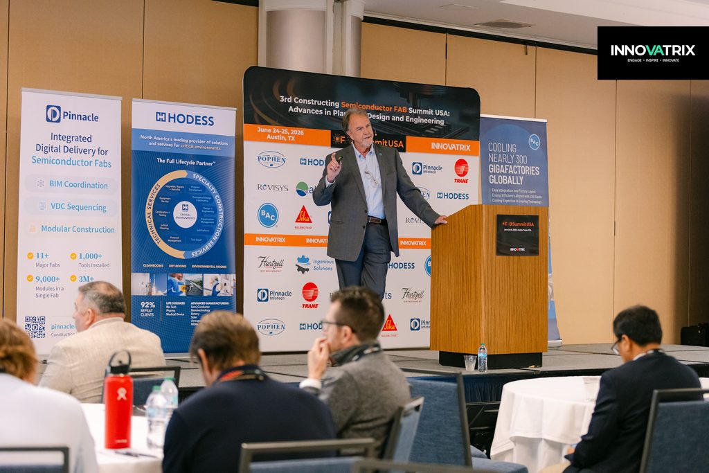
From Fab Construction to Production Ramp: A Process Engineer’s View of What Must Go Right
William Clavijo, Principal Etch Process Engineer at NXP Semiconductors

William explored the challenges of transitioning semiconductor fabrication facilities from construction completion to stable, high-volume production, emphasizing that installed capacity does not automatically translate into qualified, repeatable output. He explained that production delays often arise from unresolved process windows, tool-to-tool variation, unexpected interactions during initial production runs, and insufficient sustainment practices. He distinguished between tool installation, which establishes physical capacity, and tool qualification, which requires chamber matching, stable critical dimension and defect performance, and repeatability across shifts and maintenance cycles. He also highlighted common sources of process instability, including chamber conditioning, preventive maintenance drift, recipe sensitivity, and variations within and between chambers. To reduce these risks, he recommended structured design of experiments, statistical process control, advanced process control, and automated exception reporting. Drawing on experience across high-volume manufacturing programs, he shared results including a 29% throughput improvement, a 40% reduction in defect density, and 156 engineering hours saved per week through automation and improved data visibility. He emphasized five priorities for accelerating production ramp: involving process engineers early, defining qualification milestones, establishing control plans before initial production lots, implementing data systems from day one, and planning for ongoing equipment and process sustainment. He concluded that a fab is truly production-ready only when its processes, equipment, data, and people are aligned to deliver consistent, stable output.
Forward-thinking delivery strategies in an evolving semiconductor industry
Cameron E. Meyer, Global Semiconductor Market Director at Victaulic

Cameron examined how semiconductor construction strategies must evolve to address increasingly complex delivery challenges, highlighting the industry’s progress in shifting from sequential to parallel execution and incorporating supply chain considerations into design. However, he argued that early integration remains a significant weakness, with designs frequently becoming fixed before key project stakeholders are involved, limiting opportunities to influence decisions and increasing the cost of later changes. He identified skilled craft labor as one of the industry’s most overlooked constraints, pointing to growing workforce shortages and the impact of labor availability on project delays. He also highlighted two critical infrastructure challenges: power and water. Semiconductor facilities increasingly compete with AI data centers for electrical equipment, while transformer shortages and lengthy grid interconnection queues threaten project schedules. At the same time, high water consumption and the growing number of fabs in water-stressed regions make sustainable water management essential. Cameron proposed a resource-first approach to future fab development, incorporating on-site power generation, water reclamation, closed-loop reuse, and shared infrastructure across semiconductor megasites. He also emphasized designing facilities around actual resource availability and reducing demand through greater efficiency and reuse. He concluded that the next decade of semiconductor construction will require more than faster delivery; it will demand fundamentally different approaches to planning, siting, and resource management.
From Reactive to Resilient: AI-driven Data Strategy for Semiconductor Fabs
Deepshikha Sekhawat, Business Intelligence Program Manager at AMD

Deepshikha explored how AI-driven data strategies can strengthen semiconductor supply chain resilience amid unprecedented industry growth, geopolitical uncertainty, and increasing demand for advanced manufacturing capacity. She introduced a five-part resilience framework: Plan, Predict, Prepare, Protect, and Perform, supported by risk mitigation, cost optimization, and predictive intelligence. She highlighted the importance of supplier visibility, dual sourcing, and strategically reserved inventory, explaining how targeted PACE inventory planning helped maintain production during COVID-19 lockdowns and supplier factory incidents. She also outlined an automated purchase price variance approval process designed to improve cost control, financial governance, and compliance, including global deployment and training for more than 740 users. Drawing on experiences involving a factory fire, Hurricane Harvey, and pandemic-related disruptions, Deepshikha demonstrated how structured business continuity planning, alternative suppliers, logistics coordination, and regular status updates enabled rapid responses while protecting production. She emphasized that the next stage of supply chain resilience lies in moving beyond reactive crisis management towards predictive intelligence, using advanced analytics, machine learning, and integrated data platforms to identify risks earlier. She concluded that lasting resilience depends on data visibility, diversified sourcing, effective cost governance, and adaptable digital operations.
Spend Less, Save More: How Optimal Chiller Plant Design Creates OPEX & CAPEX Savings
Matt Travis, Advanced Manufacturing Manager at Trane

Matt explained how optimal chiller plant design can reduce both capital expenditure and ongoing operating costs while supporting the semiconductor industry’s commitment to achieving net-zero greenhouse gas emissions by 2050 and cutting emissions by 43% from 2019 levels by 2030. He emphasized that early design decisions, including supply temperature, temperature differential (Delta T) and flow rate, have a lasting impact on construction costs and energy consumption through their influence on pump, pipe, fan and duct sizing. He highlighted how series chiller configurations and higher Delta T can reduce system lift and improve efficiency, with one example demonstrating a 14% reduction. He also showed how selecting larger 4,000-ton chillers rather than 2,000-ton units for a 20,000-ton plant could halve the number of chiller bays and reduce required chiller space by 23%, saving approximately $1.3 million at an assumed construction cost of $2,000 per square foot. Across the wider plant, optimized designs could deliver pump energy savings of 22–24%, piping material savings of 13–14%, chiller and cooling tower savings of up to 46%, and heat recovery savings of 80%. Matt concluded that achieving meaningful emissions and cost reductions requires early collaboration with suppliers, smarter system design, higher Delta T and greater use of recovered heat rather than simply rejecting it.
Design for Ergonomics in the Semiconductor Industry
Paul Schwab, Principal at Ergo Design Guide

Paul highlighted the importance of integrating ergonomics into semiconductor facility and equipment design to protect worker health, improve productivity and reduce the risk of injury. Although the industry’s injury rate is significantly lower than that of manufacturing as a whole, ergonomics-related factors accounted for approximately 36% of injuries resulting in days away from work at U.S. semiconductor device manufacturing sites in 2020. Common risks include heavy lifting, awkward maintenance postures, repetitive assembly tasks and prolonged computer use. He explained that effective ergonomics delivers benefits beyond safety, including improved product quality, worker efficiency and retention, reduced defects and increased production output. While automation can reduce repetitive work and manual handling, it can also introduce new risks when equipment is designed around robots rather than human operators. Paul advocated addressing ergonomic considerations early, before equipment is purchased or installed, as retrofits are often difficult and costly. He outlined practical measures such as lifting aids, suitable storage heights, adjustable workstations and adequate rest breaks, alongside relevant regulatory requirements and industry standards. He also emphasized the value of SEMI S8, which provides established ergonomic design criteria for semiconductor equipment, and the need to consider operational access requirements beyond the equipment’s stated footprint. He concluded that successful ergonomics programmes require early design involvement, ongoing evaluation and commitment across the organization.
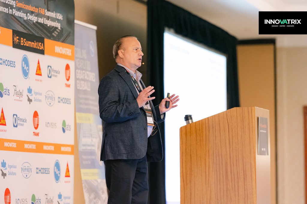
How to Utilize Innovative Construction Materials to Build Semiconductor Facilities 30%-40% Faster and MUCH SAFER
Jim Chilinski, Vice President – Strategic Projects & Accounts at Sika Corporation

Jim examined how innovative construction materials can accelerate semiconductor facility delivery while improving safety, sustainability and labor efficiency amid growing workforce shortages. He highlighted three key developments: synthetic fibers replacing steel reinforcement in concrete slabs and decks, 3D concrete printing, and insulated metal roof panels. Synthetic fibers can reduce installation time and labor requirements, improve crack and curl control, ensure reinforcement is correctly positioned throughout the concrete, and potentially cut CO₂ emissions by up to 86%. He also addressed challenges associated with Type 1L cement, including slower strength gain, difficult finishing and reduced abrasion resistance. He presented a polishable dry-shake hardener solution designed to overcome these issues, allowing floors to be polished after seven days rather than 30–60 days, accelerating polishing by up to 80% and delivering durable, dust-free surfaces suited to cleanroom environments. Jim also explored 3D concrete printing systems, which integrate robotic or gantry equipment, software and specialized concrete mixtures. Turning to roofing, he emphasized the importance of durability, fire and weather resistance, sustainability and long-term performance in mission-critical facilities. He showcased integrated solar roofing and insulated roof deck systems that reduce installation steps, material requirements, labor exposure and construction time while improving energy efficiency. He concluded that adopting innovative materials early can deliver faster, safer and more sustainable semiconductor construction without compromising facility performance.
Building Around the Tool: Strategies for Early Set Success and Production Ramp
Jennifer Ahrens, Project Director – Advanced Facilities Group, and Alikie Counihan, Engineering Project Manager, at Sundt Construction

Jennifer and Alikie explored how early coordination between construction, facility design and factory teams can accelerate equipment installation and production ramp while balancing competing project priorities. They highlighted the challenge of meeting owners’ expectations for rapid returns on investment, factory managers’ demands for high output and yield, and facility operations’ need for reliable, zero-downtime environments, particularly as process technology and tool layouts continue to evolve. They emphasized the importance of establishing clear governance, accountability and decision-making structures involving facility operations, construction and design, factory layout, factory management and tool installation teams. Through close partnerships and flexible build sequencing, they demonstrated how phased delivery of mechanical, cleanroom and support facility space, together with early turnover of critical systems and installation crews, can accommodate changing tool requirements without unnecessarily disrupting construction. They also introduced the CHUM governance forum, built around open communication, partnership with experts and collaboration to develop effective solutions. Another key focus was BIM-based space management, which requires more than simply coordinating teams in a model. Effective governance needs clear leadership, compliance oversight and field accountability, particularly in congested areas where multiple activities must proceed in parallel. Finally, they highlighted the value of standardization and modularization in tool layouts and interconnections to reduce variability, minimize errors and support predictable installation and performance.
Sustaining and upgrading a legacy facility
Charles Hogan Jr, Assoc. Director of Strategic Accounts & Custom Success at Pinnacle Infotech

Charles explored how building information modeling (BIM), modular construction and digital technologies can help sustain and upgrade legacy semiconductor facilities while accelerating project delivery. He emphasized that every stage of engineering, procurement and construction operates against the same deadline, with design changes, long-lead equipment, congested sites and cleanroom restrictions creating significant risks to schedules and costs. He demonstrated how coordinated BIM models improve planning, identify clashes before construction, manage design changes and provide more reliable fabrication packages. Reported outcomes included a 25% reduction in rework, 18% cost savings through prefabrication and coordination across more than 15 disciplines. He also highlighted model-based quantity takeoffs, 4D/5D simulations and early vendor engagement as ways to improve procurement certainty and reduce change orders. Modular construction enables mechanical skids, pipe racks, utility corridors and other components to be fabricated offsite in parallel with base-building work, reducing site congestion, installation time and labor requirements. During construction, virtual design and construction (VDC) supports installation sequencing, crane logistics, material flow and area handovers, helping teams avoid conflicts and maintain progress. Looking ahead, Charles identified AI-assisted clash detection, automated routing, robotics, reality capture and predictive project controls as important developments. He concluded by showing how coordinated BIM models can evolve into operational digital twins, supporting asset management, preventive maintenance, facility monitoring and capacity planning.
Workforce Development for Texas Semiconductor Facilities
Clayton Huber, Director, Workforce Development at Texas A&M Semiconductor Institute

Clayton highlighted the importance of workforce development in supporting Texas’s rapidly expanding semiconductor industry, which has attracted more than $76 billion in announced private investment since 2021 and supports over 47,000 semiconductor jobs. As fab construction accelerates, he identified workforce capacity as a critical factor influencing project schedules and delivery risks. Key challenges include an aging workforce, competition from adjacent industries, shortages of skilled tradespeople and technicians, and a lack of semiconductor-specific safety and cleanroom knowledge. He also highlighted fragmented education and industry pathways, with traditional training often failing to prepare workers for the specialized requirements of semiconductor facilities. Clayton outlined a workforce development approach built around industry-informed education-to-employment pathways, stackable training modules, accelerated upskilling and public-private collaboration. Training should begin with actual industry roles and align curricula with construction, facilities and equipment installation requirements, incorporating practical knowledge of cleanroom protocols, fab safety, OSHA standards, ultra-pure water systems and gas delivery. He presented the Texas A&M Semiconductor Institute as a convener of industry, education and government, helping employers develop fab-ready talent, access state and federal workforce funding, and expand training capacity. He concluded that workforce development must be treated as shared infrastructure, planned as deliberately as the semiconductor facilities themselves.
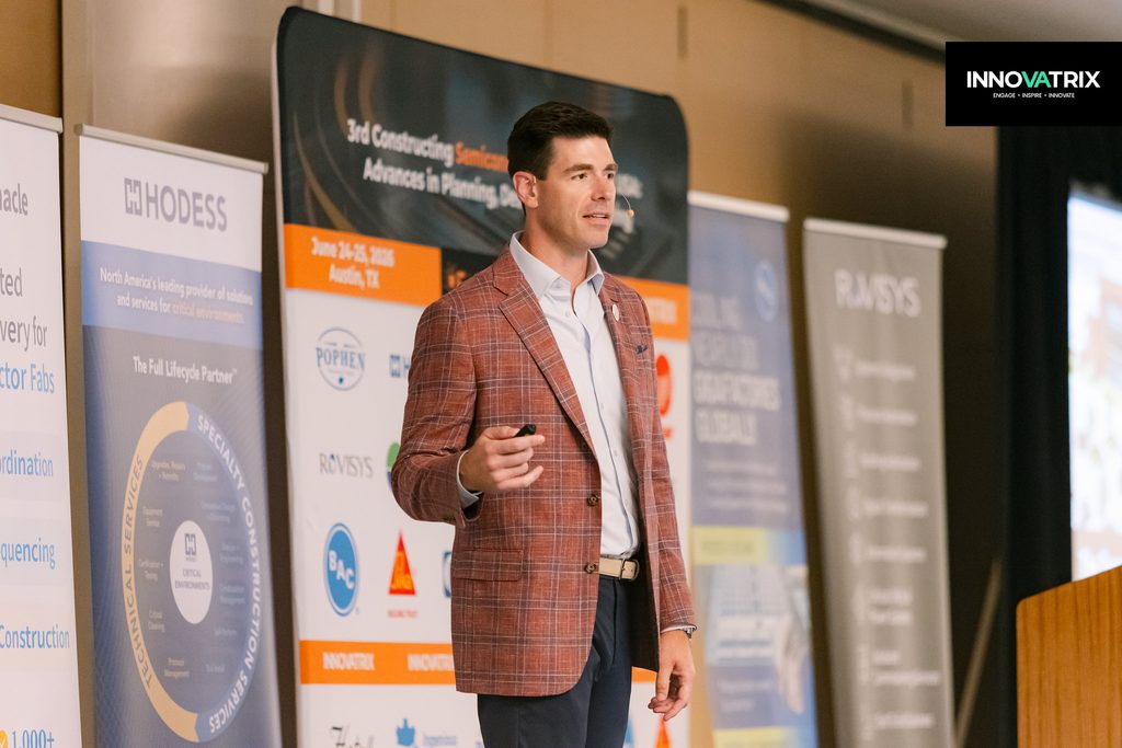
Let’s Rethink TI Across The Industry
Adib Sabet, Global Tool Install Engineering Manager at Intel Corporation

Adib challenged the semiconductor industry’s project-by-project approach to tool installation, arguing that its inefficiencies are rooted in a structural business model rather than simply poor execution. Although the same tool platforms, suppliers and engineering requirements are repeated across multiple fabs, installation methods and utility connections are frequently redesigned for each site. This leads to duplicated engineering, additional handoffs, inconsistent results and delays that affect production start-up, revenue and capacity. He highlighted the misalignment between owners seeking faster delivery and suppliers rewarded for completing individual project scopes rather than developing solutions that deliver benefits across multiple facilities. Adib argued that the industry needs to move from project-specific installations towards standardized, platform-level solutions that can be developed once and deployed across different fabs and owners. This requires changing supplier expectations and incentives, establishing consistent installation requirements, capturing lessons learned and measuring success through schedule improvements, reduced rework and business outcomes. He also called on suppliers to take greater ownership of developing scalable solutions rather than relying on owner-led decisions for every project. He concluded that the industry already has the necessary expertise and supplier capabilities but lacks a shared delivery model. Starting with one common tool platform, proving the approach and scaling it across the industry could create more consistent performance, faster installations and a sustainable competitive advantage.
Driving Predictability in Semiconductor Capital Projects
Kristin Homsi, Manager of Supply Chain at Bechtel Corporation

Kristin examined how integrated engineering, procurement and construction (EPC) delivery can improve predictability in increasingly complex semiconductor capital projects. She highlighted three major challenges: growing pressure to bring facilities online quickly, frequent changes to products and designs during construction, and unprecedented project scale and complexity. She stressed the financial importance of schedule certainty, noting that a six-month schedule change can result in more than $2 billion in additional or lost revenue. Kristin advocated a programmatic, integrated EPC approach that connects engineering, procurement, construction, commissioning and project management through a shared source of truth. This enables teams to manage change more effectively, align design with construction and commissioning requirements, and optimize total installed costs. She outlined the importance of detailed project controls, including critical-path scheduling, real-time progress reporting, cost and schedule monitoring, and collaborative change management. A principled supply chain strategy was another key priority, incorporating early supplier engagement, strategic sourcing, long-lead procurement, supplier development, risk management, sustainability and modularization. She also highlighted the role of digital tools in improving visibility and coordination, including model-based workflows, Advanced Work Packaging, drone-enabled site monitoring and extended reality visualization. By linking project models with engineering, procurement and construction data, teams can track progress and respond to changes more effectively. She concluded that integrated delivery, strategic supply chain planning and digital visibility are essential to achieving faster, safer and more predictable project outcomes.
Cross-Disciplinary Collaboration in Fab Construction: Utilizing LEAN Thinking to align people, work, information, processes, and decisions in Semiconductor Fab Construction
Sanjukta Sunny Chatterji, Job Engineer at Hensel Phelps

Sanjukta highlighted the coordination challenges facing semiconductor fab construction, including compressed schedules, labor shortages, trade congestion, supply chain constraints, late design changes, regulatory complexity and safety requirements. She emphasized that coordination failures can affect not only construction progress but also manufacturing readiness. With semiconductor investment and demand expected to grow significantly, she argued that better construction management practices are essential. She advocated Lean Construction Management as a way to treat construction as an integrated production system focused on maximizing value, improving workflow and reducing waste. Key approaches include Integrated Project Delivery (IPD), which brings owners, designers, contractors and trade partners together early around shared, measurable goals and collective accountability. She outlined practical Lean tools such as pull planning, the Last Planner System, Gemba walks, just-in-time delivery and root cause analysis. These methods help teams identify constraints, improve handovers, coordinate material flows, reduce rework and create more reliable schedules. Sanjukta also stressed the importance of a respectful, collaborative culture in which every team member can contribute to improvements, regardless of role or seniority. However, she cautioned that Lean implementation depends on strong leadership, effective training, trust and collaborative contractual arrangements.
Off-Site Manufacturing Techniques For Semiconductor Cleanroom Construction
John Dunn, US Director Off-Site Manufacturing at Exyte US Inc.

John explored how off-site manufacturing (OSM) can help address supply chain constraints and reduce construction schedules in semiconductor cleanroom projects. He outlined its key benefits, including improved safety and quality, reduced reliance on skilled labour, shorter schedules, better site logistics and the potential for capital expenditure savings. Successful implementation, however, requires customer investment, alignment with Authorities Having Jurisdiction (AHJs), OSM-ready design documentation and available supply chains. He presented several cleanroom innovations, including advances in filter fan units (FFUs), specialised plenum-integrated and return-air solutions, and ExyVision, a browser-based 3D design tool that supports customer collaboration, product visualisation and operator training. Modular cleanroom ceiling and support-area solutions, such as the 24-by-8-foot grid module and 40-by-8-foot ExyCell, integrate multiple components off-site to reduce on-site labour, working at height, supports and installation time while improving quality. John also highlighted modularisation of subfab and process utilities, covering engineering, procurement, fabrication, logistics, installation and commissioning. Digital platforms support this process by connecting design, procurement, inventory, quality, scheduling, progress and handover information. Finally, he discussed global integration facilities and project-tracking technology that uses digital site data, AI-enabled analysis and integrated dashboards to improve visibility and coordination throughout delivery.
Sponsors
The 3rd Constructing Semiconductor FAB Summit USA was supported by a wide range of sponsors who brought their teams to our exhibition hall, and Innovatrix would like to thank them again for their support.
Pophen, Hodess, BAC, Sika, Pinnacle Infotech, Trane, RoviSys, ATS Duct, Hartzell Air Movement and Ingenious Solutions.

If you want to attend our next construction summit and have the opportunity to hear presentations like these and many more, join us for the 2nd Pre-construction for Mega Facilities Summit USA, taking place March 16-17, 2027, in Dallas, Texas, USA, and explore how modern technologies and strategies are transforming planning, design, and project delivery.
For more information, visit our website or email us at info@innovatrix.eu for the event agenda. Visit our LinkedIn to stay up to date on our latest speaker announcements and event news.