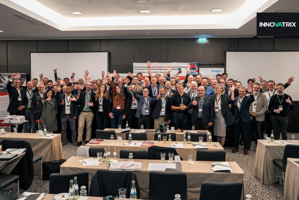
The 2nd Constructing Semiconductor FAB Summit Europe: Advances In Planning, Design And Engineering took place from October 21-22, 2025, at the Eurostars Grand Central Hotel in Munich, Germany. The two day conference provided a platform to explore cutting-edge fab construction, automation, operation, cleanroom design, and sustainability strategies helping to accelerate projects, optimize costs, and future proof the industry.
Our attendees explored the cutting-edge innovations in semiconductor plant design, fast-tracking fab construction projects, next-generation equipment integration in semiconductor fabs, critical requirements for building fabs, best practices for cleanroom certification and validation, modular construction and prefabrication trends, strategies for effective cost control in high-stakes projects and cross-disciplinary collaboration in fab construction.
This article will provide a session recap for those who didn’t get the chance to attend and serve as a reminder for those who attended.
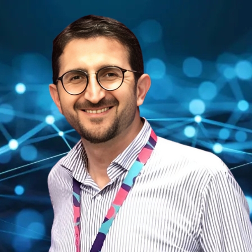
Essential chips made globally, trusted in Europe
Manfred Horstmann, General Manager & Senior Vice President at GlobalFoundries

Manfred outlined how GlobalFoundries is strengthening Europe’s semiconductor manufacturing capabilities through a globally connected yet locally focused production strategy. He explained how the company combines a unified design ecosystem, proven technologies and broad IP support to enable scalable and secure manufacturing across international markets.
A major focus of the keynote was the continued expansion of GF Dresden, described as Europe’s largest foundry. Manfred highlighted the site’s extensive cleanroom and laboratory facilities, advanced chip technologies and role within the Silicon Saxony cluster. He also discussed the company’s plans to increase production capacity between 2020 and 2027 to support automotive and critical infrastructure demand, marking the fastest and largest expansion in the company’s history.
The presentation also explored Europe’s secure FDX manufacturing flow, covering everything from design to packaging and testing. Manfred emphasised applications in aerospace, defence and secure infrastructure, alongside the importance of trusted, ITAR-free production.
He concluded by showcasing the GlobalShuttle MPW programme, which enables cost-effective prototyping and accessible innovation for start-ups, universities and industrial partners, while supporting the future development of next-generation FD-SOI technologies for edge AI and quantum computing.
High basic energy & media consumption of semiconductor factories, even without being productive
Thomas Quarg, Director Facility Management & Infrastructure at ams-Osram International GmbH

Thomas focused on the challenge of reducing the substantial baseline energy consumption within semiconductor fabrication plants, noting that a large proportion of energy and media usage occurs even when no wafers are being produced. His keynote explored practical methods for measuring, analysing and optimising consumption across fab operations.
He explained the importance of establishing accurate energy monitoring systems, including the installation of static and flexible meters connected to a central facilities database. Thomas highlighted how detailed, real-time data collection enables more effective analysis of utilities such as electricity, water, gases and cooling systems.
A key theme was the development of “golden tools” – representative production systems used to model and simulate energy consumption across identical equipment. By integrating production utilisation data with energy monitoring through APIs, digital dashboards and analytics platforms, manufacturers can identify inefficiencies and uncover opportunities for savings.
Thomas also examined energy behaviour during fab shutdowns and maintenance periods, demonstrating how idle consumption can be significantly reduced through targeted operational measures. He stressed that underutilised production periods should be treated as opportunities to improve efficiency strategies.
The presentation concluded with a forward-looking discussion on digital twins, machine learning and predictive maintenance, with the goal of creating smarter, more energy-efficient semiconductor facilities.
Asia meets Europe – Comparison of technical requirements and conditions in the Semiconductor Environment
Tobias Frieser, Head of Business Development Europe at Pophen (L&B International)

Tobias delivered a comparative overview of semiconductor construction projects across Asia and Europe, focusing on cleanrooms, dry rooms, permitting procedures and regulatory frameworks. Drawing on examples from China, Thailand, India and Germany, he highlighted how regional differences can significantly influence project timelines, processes and costs.
He explained the key authorities and approval stages involved in each market, including environmental, fire safety, occupational health and equipment certification requirements. Tobias noted that Thailand and China often offer the fastest permitting pathways, particularly within industrial estates and special economic zones, while Germany and India can involve longer approval periods due to more complex or sequential regulatory procedures.
Despite these differences, Tobias stressed that many of the technical regulations and standards governing clean and dry room environments remain broadly aligned across regions. He encouraged delegates to adopt a global perspective and learn from international best practice, while still recognising the importance of local conditions and project-specific requirements.
The keynote concluded with the message that every semiconductor construction project is unique, shaped by regional mindsets, regulations and operational approaches. Tobias emphasised that international suppliers can play an important role in bridging these differences by combining global experience with local project support.
Project Management Effectiveness in the Semiconductor Industry Towards Product Release
Daniela Marum, Team Leader – Project Management for Industrial Engineering at Nexperia

Daniela explored the growing complexity of project management within the semiconductor industry, highlighting the need to balance time, quality and budget in an environment where even a single day of fab shutdown can result in losses of approximately $100 million. Her keynote focused on practical, field-tested approaches to improving collaboration, communication and team performance across large-scale industrial projects.
She examined the use of both agile and waterfall project management methodologies, explaining how each can support semiconductor operations depending on project scope and requirements. Daniela stressed that the rapid growth and increasing importance of the industry have made effective stakeholder management more critical than ever.
A major theme of the presentation was the importance of clear communication between customers, suppliers, internal departments, governments and investors. Daniela encouraged delegates to provide concise, structured information, maintain regular follow-up and clearly define expectations to improve efficiency and reduce risk.
She also addressed cross-site collaboration, emphasising the value of shared goals, transparent communication, clearly defined roles and the use of technology to maintain alignment across teams.
Concluding with team motivation, Daniela highlighted the importance of trust, recognition, empowerment and active listening in building resilient and high-performing project teams within the fast-paced semiconductor sector.
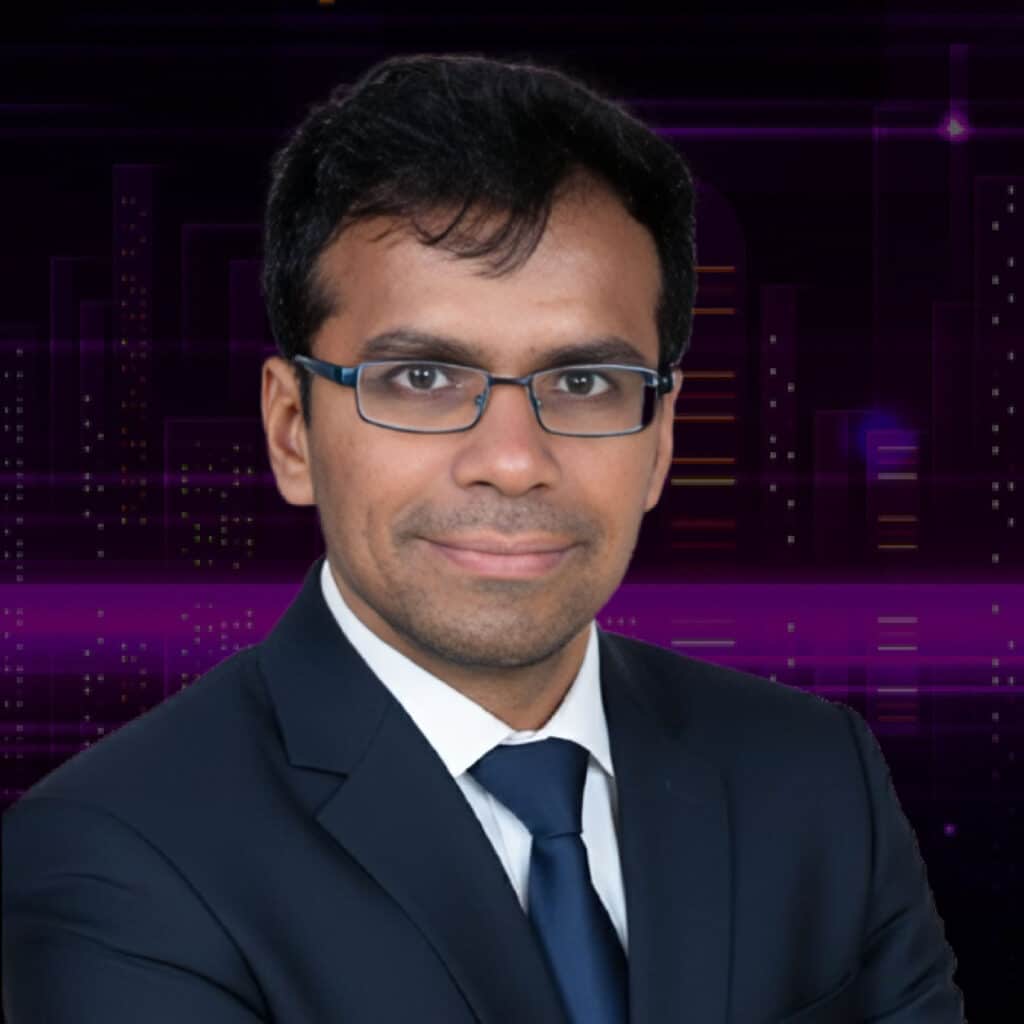
Quantum-Inspired ML for Semiconductor Manufacturing
Paul Satinder, Chief Technology Officer at Hermes Semiconductors Pvt Ltd

Paul explored how quantum-inspired machine learning can enhance semiconductor manufacturing by applying quantum computing principles through classical hardware to solve complex production challenges more efficiently. His keynote focused on the practical application of advanced analytics to improve yield, reduce downtime and optimise fab operations without waiting for full-scale quantum computing technologies.
The presentation centred on three core areas: defect detection, process optimisation and predictive maintenance. Paul explained how AI-driven vision systems can identify subtle defect patterns earlier, reduce false alarms and improve first-pass yield through faster and more accurate inspection processes. He also highlighted how adaptive process optimisation can minimise variability across lithography, etching and deposition stages, helping manufacturers achieve more consistent wafer quality while lowering costs.
A further focus was predictive maintenance, where machine learning models analyse equipment data such as vibration, temperature and flow signals to anticipate failures before they occur. Paul demonstrated how this approach can reduce unplanned downtime, improve overall equipment effectiveness and extend asset life.
He also addressed implementation strategies, including phased deployment, data governance and workforce upskilling. Concluding the session, Paul positioned quantum-inspired machine learning as a practical manufacturing tool capable of delivering measurable improvements in yield, uptime and operational efficiency today.
Air Filtration Solutions for Microelectronics Facilities
Mike Sehgal, Global Director High Purity Segment Microelectronics & EV Battery at AAF International

Mike presents AAF International’s comprehensive approach to clean air solutions across industries. As a subsidiary of Daikin Industries since 2006, AAF operates globally with over 5,100 employees across 27 manufacturing sites, serving more than 130 countries.
The presentation emphasises AAF’s three core values: trust and transparency, drive and dedication, and unity and understanding. The company delivers integrated filtration solutions both inside and outside manufacturing facilities, addressing contamination from make-up air, pods, construction materials, operators, abatement systems, spills, and process tools.
Key product portfolios include high-purity solutions such as MEGAcel® HEPA/ULPA filters and AstroFan filter units for microelectronics cleanrooms, alongside gas-phase filtration systems and specialised equipment. AAF also provides advanced monitoring technology through Sensor360® and comprehensive total cost of ownership analysis via VisionAir® TCO.
The company distinguishes itself as a complete one-stop-shop by combining Daikin’s air handling capabilities with AAF’s filtration expertise, supported by six global R&D centres. Services encompass facility audits, predictive maintenance, and total filter management, positioning AAF as a trusted partner for microelectronics manufacturers seeking integrated, high-performance air quality solutions.
Strengthening the Design-for-Test Bridge: Enabling Cost-Effective Semiconductor Manufacturing with Actionable Data
Hans Martin von Staudt, Director Design-for-Test at Renesas Electronics

Hans explored the critical role of Design-for-Test (DfT) in modern semiconductor manufacturing, highlighting how it acts as a bridge between design engineering, manufacturing and test operations. His keynote examined how increasingly complex semiconductor devices require advanced testing strategies to maintain yield, control costs and generate actionable production data.
He explained that every device moving through the fab should effectively function as a sensor for understanding design-process interactions. Since many process sensitivities only become visible through downstream test results, Hans stressed the importance of feeding test data back into design and manufacturing workflows to enable process adjustments, design refinements and improved reliability.
A major focus of the session was the evolution of DfT as a response to rising testing costs driven by Moore’s Law and growing product complexity. He demonstrated how digital DfT techniques have enabled faster and more parallelised testing, while mixed-signal applications increasingly rely on trimming and calibration to meet demanding performance specifications.
Hans also highlighted the value of generating parametric and diagnostic data rather than simple pass/fail outcomes. Examples from trimming and non-volatile memory testing illustrated how detailed self-test information can reveal hidden process drift and manufacturing issues.
Concluding the keynote, he discussed the importance of engineering data backbones and AI-supported analytics in enabling more intelligent process optimisation and yield improvement across semiconductor production.
From Cleanroom to Culture: Building Strong Fab Teams
Udi Gavish, Head of Global Tool Install Engineering at Intel Corporation

Udi delivered an inspiring keynote on leadership, culture and personal growth within the highly demanding environment of semiconductor construction. Using Plato’s allegory of the cave and the comfort zone model as guiding concepts, he encouraged delegates to challenge established thinking, embrace uncertainty and view discomfort as a pathway to innovation and development.
He examined the unique pressures of semiconductor construction, including complex infrastructure, tight timelines, safety risks, regulatory demands and global workforce coordination. Despite the industry’s disruptive nature, Udi argued that comfort zones still exist and that growth comes from deliberately stepping beyond them through continuous learning, reflection and collaboration.
A major focus of the presentation was motivation and workplace culture. Drawing on theories such as Carol Dweck’s growth mindset and Herzberg’s hygiene factors, Udi highlighted the importance of psychological safety, empowerment, recognition and leadership commitment in building high-performing teams. Safety was presented as the foundation of operational excellence, supported by strong communication, accountability and continuous education.
Udi also explored the evolution of leadership within semiconductor engineering, stressing that technical expertise alone is no longer enough. He advocated for emotionally intelligent, inclusive and strategically minded leaders capable of inspiring teams, driving innovation and aligning organisational goals with individual purpose in fast-paced manufacturing environments.
Leading at the Speed of Change: Driving Projects Smarter and Faster
Andreea Rasoga, PMO Operations Manager at NXP Semiconductors

Andreea explored how semiconductor organisations can improve project execution by strengthening leadership during periods of constant change. Her keynote focused on the hidden operational bottlenecks that slow down semiconductor projects, including stakeholder resistance, late alignment, unclear scope definition and delayed decision-making.
She explained how these issues often lead to rework, increased costs and project delays, even in highly advanced technical environments. According to Andreea, successful project delivery depends not only on processes and technology, but also on the ability of leaders to align people, create ownership and maintain momentum throughout change initiatives.
The presentation introduced a four-part leadership framework designed to help organisations operate more effectively under pressure: Sense, Translate, Decide and Embed. Andreea described how proactive leaders identify early warning signs, encourage cross-functional collaboration and use lessons learned to prevent recurring risks. She also emphasised the importance of translating change into clear business objectives so that teams, suppliers and stakeholders understand both the purpose and expected outcomes.
A further focus was decision-making efficiency, with recommendations for clear ownership structures, focused decision forums and faster escalation pathways. Concluding the session, Andreea highlighted the importance of embedding continuous improvement into organisational culture through learning, accountability and openness to calculated risk-taking, reinforcing the idea that while change is unavoidable, operational velocity remains a leadership choice.
“Moving the Dial” with advanced analytics in FAB Mega projects – A Framework for Effective & Predictive Analytics
Yuval Bergman, Semicon Head of Data and Analytics at Arcadis

Yuval discussed how predictive and effective analytics can help semiconductor organisations mitigate risk and improve decision-making, while emphasising that success depends on structured implementation rather than “magic” technology solutions. His keynote focused on the common barriers that prevent analytics programmes from delivering meaningful business value.
He identified several major roadblocks, including poor executive alignment, fragmented data sources, operational silos, unclear data ownership and an overreliance on lagging performance indicators. Yuval stressed that organisations often focus on symptoms instead of underlying causes, limiting the effectiveness of analytics initiatives.
To address these challenges, he introduced the SODA framework, built around four interconnected pillars: Strategy, Operation, Data and Analytics. He explained how strong executive sponsorship, clear stakeholder alignment and defined KPIs create the strategic foundation for analytics-driven projects. Operationally, he highlighted the importance of cross-functional collaboration, clear responsibilities and integrated data communities to eliminate hidden dependencies and information gaps.
Yuval also emphasised the need for trusted and standardised data through strong governance, single sources of truth and data quality controls. On the analytics side, he encouraged organisations to prioritise actionable insights, leading indicators and business-focused storytelling.
The session concluded with practical examples of how the SODA framework can support semiconductor construction and manufacturing, including capacity forecasting, trend identification and the detection of hidden project dependencies.
Fast-Track Fab: Building a High-Impact Semi Facility in Record Time
Stanley van den Heever, Director of Industrial Engineering, and Iain Docherty, Vice President of Manufacturing Operations, at Pragmatic Semiconductor

The presentation explored how semiconductor fabs can be designed and constructed for rapid deployment, scalability and operational efficiency. A major focus was the relationship between fab layout, modular construction and accelerated project delivery in response to growing global semiconductor demand and increasingly short innovation cycles.
The speaker outlined the design of a compact, modular fab built within an existing single-storey structure, using raised floors and external plantrooms instead of a traditional subfab. The layout was intentionally designed for flexibility, enabling future expansion through demountable walls, scalable services and adaptable overhead transport systems. Rather than following conventional tool layout approaches, the fab uses self-contained “mini-fabs” with short transport distances to improve efficiency and simplify operations.
The keynote also examined the importance of defining high-impact project goals centred around rapid time-to-first-wafer, cost efficiency and operational readiness. Early stakeholder alignment, phased scope definition and shared KPIs were highlighted as critical factors in reducing delays and improving execution.
Further discussion focused on modular construction methods, parallel workstreams and close vendor coordination to compress construction timelines. The speaker also addressed process enablement strategies such as early tool startup, loop lot testing and cross-site recipe sharing to accelerate qualification and production ramp-up.
Concluding the session, the presentation outlined a vision for “Fab-as-a-Service”, where modular fabs could be deployed on customer sites in under 12 months to rapidly expand manufacturing capacity.
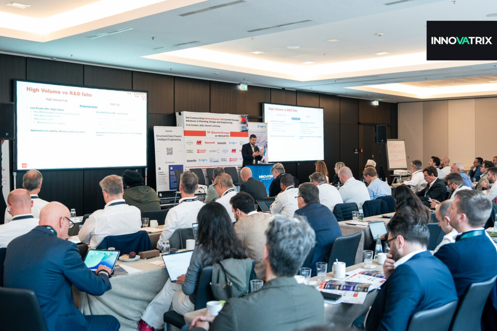
Embracing the challenge of scheduling and automation in R&D
Vincent Fischer, IT & Planning Section Manager at CEA-Leti

Vincent explored the unique operational challenges of semiconductor R&D fabs, highlighting how they differ fundamentally from high-volume manufacturing facilities in terms of flexibility, process variability and human involvement. His keynote focused on how scheduling and automation strategies must adapt to environments driven by experimentation rather than standardised production.
He explained that while high-volume fabs prioritise stability, repeatability and highly automated operations, R&D fabs manage a very high mix of low-volume projects, often with only a single lot per product. These environments require flexible process flows, highly skilled operators and a greater tolerance for uncertainty and variability.
A major focus of the presentation was operation scheduling in R&D environments. Vincent described how traditional scheduling approaches are often insufficient due to unpredictable process durations, equipment constraints and engineering-driven changes. To address this, CEA-Leti is developing simulation-based scheduling models that incorporate equipment performance, operator availability, stochastic process behaviour and what-if scenario analysis to better manage uncertainty and optimise cleanroom activity.
The keynote also explored a hybrid automation approach designed specifically for R&D fabs. Rather than replacing human expertise, automation acts as an assistant by performing pre-process checks, supporting recipe selection and automating MES tracking, while engineers retain final decision-making authority. Vincent demonstrated how this balance between automation and human insight enables greater operational flexibility while still improving efficiency, reliability and data traceability within research-focused semiconductor facilities.
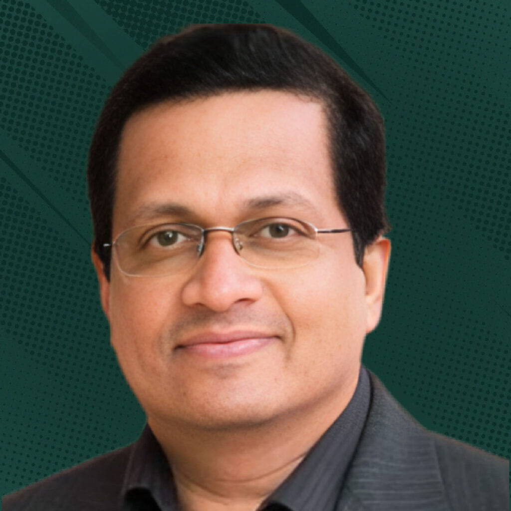
Process Engineering Challenges during Ramp-Up
Michael Friedemann, Process Manager Diffusion at Robert Bosch Semiconductor Manufacturing Dresden GmbH

Michael explored the complexity of semiconductor process engineering during production ramp-up phases, highlighting that every process ramp is unique due to differing products, substrates, equipment configurations, infrastructure and manufacturing goals. His keynote focused on the challenge of balancing productivity, quality, environmental considerations and operational constraints within increasingly advanced semiconductor environments.
He explained that modern process engineering is shaped by rapidly growing technological complexity, high power consumption demands, expanding sensor networks and vast quantities of production data. According to Michael, managing this complexity successfully requires not only advanced tools, but also a strong data-centric infrastructure combined with collaborative working methods and a digital mindset across organisations.
A major focus of the session was the use of smart manufacturing methods to improve advanced process control. Michael introduced artificial metrology, where software-based systems emulate physical metrology tools using existing digital data sources. This enables faster inline process control, supports AI-driven manufacturing and reduces dependency on physical measurement equipment.
He also presented the application of MIMO run-to-run advanced process control, where recipe parameters are dynamically adjusted based on post-metrology feedback. This approach improves process stability, reduces manual adjustments, saves test wafers and extends equipment lifetime through more efficient power management.
Concluding the keynote, Michael emphasised that data-driven IT architectures and intelligent process control methods are becoming essential for improving yield, productivity, sustainability and material efficiency in semiconductor manufacturing.
Talent pipeline development for a growing European semiconductor industry
Bernard Capraro, Senior Manager, University Partnerships and Talent Initiatives at SEMI Europe GmbH

Bernard addressed the growing talent challenge facing Europe’s semiconductor industry, highlighting projections that the sector could face a workforce gap of more than 75,000 employees by 2030. His keynote explored the disconnect between Europe’s strong STEM graduate output and the relatively small proportion of graduates entering semiconductor careers.
He explained that although hundreds of thousands of students graduate annually in semiconductor-related fields, only a small percentage ultimately join the semiconductor industry. Combined with increasing investment in European semiconductor manufacturing and a significant proportion of the existing workforce approaching retirement, this creates mounting pressure on the industry’s future talent pipeline.
A major focus of the session was the changing expectations of younger generations entering the workforce. Bernard noted that Gen Z employees place strong value on continuous learning, development opportunities and meaningful career progression. He argued that semiconductor companies must therefore create environments that support personal growth, practical learning and long-term engagement in order to attract and retain talent.
The keynote also highlighted the increasing importance of AI, data analysis and programming skills across all technical levels of the industry. Bernard encouraged stronger collaboration between education providers, governments and industry leaders to modernise STEM education through more hands-on and engaging learning experiences.
Concluding the session, he stressed that talent development should be viewed as a shared European responsibility, with greater cooperation between institutions needed to strengthen the future semiconductor workforce.
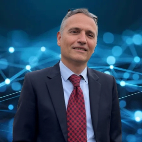
Clean room HVAC optimization
Tiziano Petrosino, Facilities & EHSS Director at LFoundry

Tiziano explored the significant energy demands associated with semiconductor cleanroom operations, focusing on how HVAC optimisation can improve both sustainability and operational efficiency within semiconductor fabs. His keynote highlighted the critical role of air quality control in maintaining production yields and the substantial energy costs linked to temperature, humidity and airflow management.
He explained that semiconductor fabs in Europe can spend tens of millions of euros annually on electricity and gas, with HVAC and cooling systems accounting for a major share of facility energy consumption. Tiziano detailed how humidity control, heating, cooling and airflow each contribute differently to overall energy demand, particularly under varying seasonal conditions.
A major focus of the session was the optimisation of chilled and condenser water systems using psychrometric principles. Tiziano demonstrated how careful adjustment of chilled water temperatures, condenser water settings and cooling strategies can significantly improve chiller efficiency and reduce operating costs. He also explored the use of free cooling systems during colder months, where external air temperatures can be utilised to cool water systems with minimal energy input.
The presentation additionally addressed practical operational improvements, including filter maintenance, exhaust optimisation and seasonal adjustments to cleanroom environmental settings. Tiziano stressed that even relatively small operational changes can deliver substantial long-term energy savings while maintaining strict semiconductor manufacturing standards.
Concluding the keynote, he outlined several key optimisation initiatives that semiconductor fabs can implement to reduce HVAC-related energy consumption, improve efficiency and support more sustainable cleanroom operations.
Protecting People & Processes: Low-Level Gas Detection for Semiconductor Fabs
Eric Jüchtzer, Senior Sales Representative at Honeywell

Eric presented an overview of gas detection technologies used within semiconductor manufacturing environments, focusing on the critical importance of identifying hazardous gases to protect both personnel and production facilities. His keynote outlined the four primary categories of gas hazards encountered in semiconductor operations: combustible, poisonous, oxygen-depleting and corrosive gases.
A major focus of the presentation was the comparison of different gas detection technologies and their suitability for semiconductor applications. Eric explained the working principles behind electrochemical sensors, where gas reactions within an electrolyte generate measurable electrical signals proportional to gas concentration. He highlighted these sensors as intelligent, cost-effective solutions widely used for detecting many common industrial gases.
The session also explored Honeywell’s Chemcassette® technology, a dry colourimetric detection system that has been widely adopted within the semiconductor industry since the 1980s. Eric described how chemically treated paper reacts with target gases to create visible colour changes, allowing highly sensitive optical measurement. He emphasised several advantages of the system, including extremely low detection limits, resistance to cross-interference from common semiconductor gases, zero drift behaviour and reliable operation even in oxygen-free environments.
Concluding the keynote, Eric stressed that different gas detection methods should be viewed as complementary rather than competing technologies. He also highlighted the importance of combining multiple sensing technologies, including FTIR, IR, NDIR, PID and UV/IR systems, to ensure comprehensive gas monitoring and safety coverage within semiconductor manufacturing facilities.
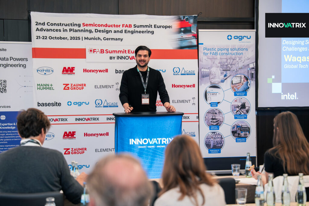
Designing SoCs for AI & Functional Safety: Challenges and Opportunities
Waqas S Jutt, Global Tech Lead Architect at Intel Corporation

Waqas explored the growing complexity of designing AI-enabled semiconductor systems for edge computing and automotive safety-critical applications, focusing on the balance between performance, power efficiency and functional safety. His keynote examined how modern AI SoCs are evolving to support increasingly sophisticated workloads while meeting strict safety and reliability requirements.
He outlined the architecture of functional safety AI SoCs, which integrate heterogeneous compute elements such as CPUs, GPUs, NPUs and DSPs alongside high-bandwidth memory systems, network-on-chip interconnects and dedicated safety islands for monitoring and diagnostics. The presentation demonstrated how data flows through AI inference pipelines while continuously being supervised by embedded safety mechanisms.
A major focus of the session was the challenge of combining AI’s probabilistic behaviour with the deterministic requirements of functional safety standards. Waqas discussed key industry challenges including complex verification processes, increased silicon and power overhead from safety features such as ECC and lockstep architectures, data integrity concerns and rising reliability risks associated with advanced semiconductor nodes.
The keynote also examined the growing influence of regulatory frameworks such as the EU AI Act and ISO/PAS 8800, which are shaping the future development of certifiable AI architectures and safety-integrated chiplet designs.
Concluding the session, Waqas emphasised the importance of adopting a “Safety by Design” methodology, where functional safety considerations are integrated from the earliest design stages through continuous FMEA and FMEDA analysis, model-based engineering and early deployment of safety IP. He highlighted that combining AI capability with robust functional safety is essential for the next generation of intelligent semiconductor systems.
KLA metrology solutions to guarantee accurate process monitoring for fast fab ramp up
Tetyana Shapoval, Technical Engagement Manager, Metrology at KLA Corporation

Tetyana explored the critical role of metrology in ensuring successful semiconductor fab ramp-up, highlighting how accurate measurement and process control directly influence yield, cycle time and manufacturing stability. Her keynote focused on the importance of reducing process variability and enabling rapid detection of manufacturing excursions during both R&D and high-volume production.
She explained that effective metrology systems accelerate yield learning by identifying process deviations early, allowing corrective actions to be implemented before large-scale production impacts occur. Tetyana stressed that even highly capable manufacturing processes remain vulnerable to excursions in critical parameters such as critical dimensions, overlay and film thickness, making comprehensive inline monitoring essential.
A major focus of the presentation was the influence of metrology precision on process control. Tetyana demonstrated how poor metrology accuracy can increase the risk of wafer lots being incorrectly classified, ultimately affecting yield and production efficiency. She noted that most semiconductor fabs continue to monitor 100% of production lots, even in highly stable processes, due to the potentially severe impact of unexpected excursions.
The session also explored the growing complexity of metrology requirements as semiconductor technologies evolve from planar devices to FinFET, Gate-All-Around and complementary FET architectures. Tetyana highlighted advanced metrology solutions developed for applications including high-k metal gate control, MRAM monitoring, GaN manufacturing and advanced packaging.
Concluding the keynote, she emphasised that metrology performance, sampling strategies and advanced process monitoring remain essential to achieving faster fab ramps, improved die yield and reduced time-to-market in increasingly complex semiconductor manufacturing environments.
How data-driven approaches can transform the design process
Andrew Jones, Director of Engineering Solutions at Basesite

Andrew explored the growing importance of structured data in semiconductor facility design and operations, focusing on how digital transformation, automation and AI are reshaping engineering workflows. His keynote highlighted the need for consistent, accessible and well-managed data to support productivity, operational efficiency and future-ready semiconductor infrastructure.
He explained that structured data enables repeatable design processes, off-site manufacturing, digital twins and augmented reality applications, while also supporting advanced automation and AI-driven optimisation. Andrew discussed how digital twins can be used not only to optimise facility design, but also to simulate operational scenarios and improve long-term asset management.
A major focus of the presentation was the semiconductor industry’s ongoing struggle to fully realise the promises of Building Information Modelling (BIM). Andrew identified several barriers that have limited adoption over the past two decades, including fragmented industry standards, inconsistent management support, resistance to change and unclear implementation goals.
The session also examined the “journey of a data point” across engineering systems, highlighting the importance of ownership, formatting, traceability and integration between tools, utility systems and control platforms. Andrew demonstrated how engineering metadata, utility distribution information and digital asset management systems can support smarter decision-making throughout a facility’s lifecycle.
Concluding the keynote, he stressed that improving the industry’s “data attitude” requires recognising data as a valuable operational asset. He encouraged organisations to define clear data requirements within contracts, tailor data strategies to each individual project and learn from the semiconductor industry’s successful adoption of safety and quality cultures to drive future digital transformation.
Cleanroom Process Integration and CMP Challenges in Advanced Semiconductor Manufacturing
Sanghamitra Ghosal, Scientist at the Fraunhofer Institute for Electronic Nano Systems (ENAS)

Sanghamitra explored how heterogeneous integration is reshaping semiconductor system design as scaling limits shift innovation from transistor scaling to advanced packaging. Her keynote focused on 2.5D and 3D integration, chiplets, and the increasing importance of packaging technologies as the central enabler of next-generation performance, density and system efficiency.
She explained that 2.5D integration allows multiple chips to be placed side-by-side on an interposer, enabling high-bandwidth memory and chiplet-based architectures, while 3D integration stacks dies vertically using TSVs or hybrid bonding to achieve ultra-high functional density and compact system footprints. Although both approaches deliver significant performance and integration benefits, they also introduce major challenges around yield, thermal management, reliability and ultra-precise bonding requirements.
A major focus of the presentation was chiplet-based design as a flexible alternative to monolithic SoCs. Sanghamitra highlighted how chiplets enable scalable, cost-efficient and heterogeneous system architectures by combining independently manufactured functional blocks such as CPUs, memory, I/O and AI accelerators into unified systems.
The keynote also addressed the growing complexity of advanced packaging, particularly in relation to cleanroom requirements, contamination control and sub-micron defect sensitivity. She emphasised that heterogeneous integration demands much tighter surface preparation standards, especially for processes such as hybrid bonding and CMP, where atomic-scale flatness and material compatibility are critical.
Concluding the session, Sanghamitra stressed that monolithic and heterogeneous integration will coexist, with future success depending on holistic surface engineering, cross-disciplinary collaboration and a deeper understanding of interactions between materials, processes and design.
Challenges and Opportunities in Building a Fab — A Case Study
Oliwer Jan Janiszewski, Project Management at JANISHEWSKI

Oliwer’s keynote focused on how complex infrastructure projects succeed or fail based on stakeholder alignment, governance discipline, and cultural intelligence. He began by outlining the importance of mapping stakeholder incentives across investors, government authorities, local communities, and NGOs. The emphasis was on understanding core motivations, identifying common ground, and building mutual gains through transparency, structured planning, and early coalition-building.
He highlighted that early support networks—both internal and external—are critical, including supply-chain partnerships, regulatory engagement, and community outreach. Regulators, he argued, should be treated as collaborators rather than gatekeepers, with shared narratives and co-developed frameworks helping to accelerate outcomes.
A central theme was the need for a “single source of truth” through integrated digital platforms, reducing rework caused by poor data flow and miscommunication. This was paired with milestone alignment, where funding, decision-making, and progress reviews are tightly linked to clear project gateways.
Oliwer also stressed communication discipline: dashboards over documents, decision-ready information, and tailored messaging for different audiences.
Finally, he explored cultural intelligence in leadership—adapting decision styles, building integration mechanisms, and treating conflict as a feedback loop rather than a failure. His key message was that success comes from aligned incentives, unified governance, and culturally agile leadership.
Water Management in Semiconductor Fab Construction: Strategies for Sustainability, Efficiency, and Risk Mitigation
Kelly Osborne, Fab Facilities Operations Sr. Staff Engineer at Intel Corporation

Kelly’s keynote explored the growing sustainability and operational challenges facing advanced semiconductor manufacturing, with a particular focus on water management in highly complex fab environments. She highlighted how increasing microchip complexity is driving more process layers, which in turn significantly raises demand on energy, water, and supporting facility systems.
A key theme was the water–energy nexus, where rising sustainability expectations must be balanced against the need for 100% manufacturing uptime, operational efficiency, and long-term business continuity. She noted that expanding fabs are placing increasing pressure on external infrastructure and heightening risks around water circularity.
Kelly broke down the main contributors to a semiconductor site’s water footprint, including wafer rinsing and abatement processes, heating and cooling systems, chemical and gas usage, waste treatment, compressed air systems, and clean air and exhaust management systems.
She then compared onsite versus offsite water treatment strategies. Offsite treatment can reduce costs but introduces compliance and quality risks, while onsite systems offer greater control and scalability but require higher capital investment and resilience planning. She stressed that both approaches depend on strong early collaboration with municipal partners.
Finally, she outlined a structured approach to water management using site-wide mapping and digital twins to optimise reclaim systems, alongside restoration initiatives such as aquifer recharge and ecosystem improvement. Her central message was that resilient water strategies depend on integration, modelling, and strategic partnerships.
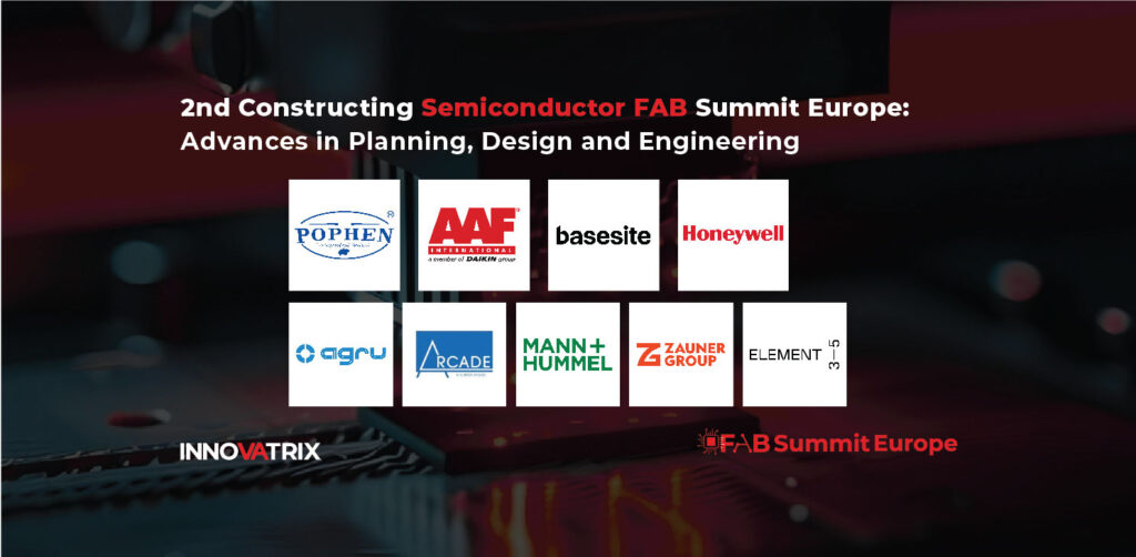
FAB Summit Europe 2025 Sponsors
The 2nd Constructing Semiconductor FAB Summit Europe was supported by a wide range of sponsors who brought their teams to our exhibition area, and Innovatrix would like to thank them again for their support.
Pophen, AAF International, Honeywell, basesite, AGRU, Arcade Engineering, Mann+Hummel, Zauner Group and element 3-5.
If you would like to network with fellow experts and innovators from across the semiconductor manufacturing industry and be informed on the latest innovations in fab construction, join us at an Innovatrix conference today! Our next European edition of the Constructing Semiconductor FAB Summit will be taking place later this year on October 21-22, 2026, in Munich, Germany.
For more information, visit our website or email us at info@innovatrix.eu for the event agenda. Visit our LinkedIn to stay up to date on our latest speaker announcements and event news.